Silicon Sleuthing: Finding A Ancient Bugfix On The 8086

Few CPUs have had the long-lasting influence that the 8086 did. It is hard to believe that when your modern desktop computer boots, it probably thinks it is an 8086 from 1978 until some software gooses it into a more modern state. When [Ken] was examining an 8086 die, however, he noticed that part of the die didn’t look like the rest. Turns out, Intel had a bug in the original version of the 8086. In those days you couldn’t patch the microcode. It was more like a PC board — you had to change the layout and make a new one to fix it.

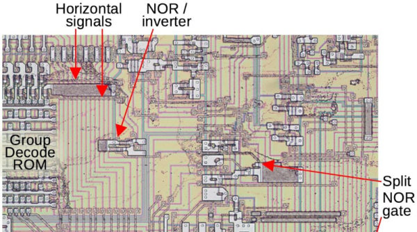
The affected area is the Group Decode ROM. The area is responsible for categorizing instructions based on the type of decoding they require. While it is marked as a ROM, it is more of a programmable logic array. The bug was pretty intense. If an interrupt followed either a MOV SS or POP SS instruction, havoc ensues.

Continue reading “Silicon Sleuthing: Finding A Ancient Bugfix On The 8086”

DIY USB Charging The Right Way

Since the widespread adoption of USB 1.1 in the 90s, USB has become the de facto standard for connecting most peripherals to our everyday computers. The latest revision of the technology has been USB 4, which pushes the data rate capabilities to 40 Gbit/s. This amount of throughput is mindblowing compared to the USB 1.x speeds which were three to four orders of magnitude slower in comparison. But data speeds haven’t been the only thing changing with the USB specifications. The amount of power handling they can do has increased by orders of magnitude as well, as this DIY USB charger demonstrates by delivering around 200 W to multiple devices at once.

The build comes to us from [tobychui] who not only needed USB rapid charging for his devices while on-the-go but also wanted to build the rapid charger himself and for the charger to come in a small form factor while still using silicon components instead of more modern gallium nitride solutions. The solution he came up with was to use a 24 V DC power supply coupled with two regulator modules meant for solar panel installations to deliver a staggering amount of power to several devices at once. The charger is still relatively small, and cost around $30 US dollars to make.

Part of what makes builds like this possible is the USB Power Delivery (PD) standard, which has enabled all kinds of electronics to switch to USB for their power needs rather than getting their power from dedicated, proprietary, and/or low-quality power bricks or wall warts. In fact, you can even use this technology to do things like charge lithium batteries.

Continue reading “DIY USB Charging The Right Way”

Dead Solar Panels Are The Hottest New Recyclables

When it comes to renewable energy, there are many great sources. Whether it’s solar, wind, or something else, though, we need a lot of it. Factories around the globe are rising to the challenge to provide what we need.

We can build plenty of new solar panels, of course, but we need to think about what happens when they reach end of life. As it turns out, with so much solar now out in the field, a major new recycling industry may be just around the corner.

Continue reading “Dead Solar Panels Are The Hottest New Recyclables”

Old Printer Becomes Direct Laser Lithography Machine

What does it take to make your own integrated circuits at home? It’s a question that relatively few intrepid hackers have tried to answer, and the answer is usually something along the lines of “a lot of second-hand equipment.” But it doesn’t all have to be cast-offs from a semiconductor fab, as [Zachary Tong] shows us with his homebrew direct laser lithography setup.

Most of us are familiar with masked photolithography thanks to the age-old process of making PCBs using photoresist — a copper-clad board is treated with a photopolymer, a mask containing the traces to be etched is applied, and the board is exposed to UV light, which selectively hardens the resist layer before etching. [Zach] explores a variation on that theme — maskless photolithography — as well as scaling it down considerably with this rig. An optical bench focuses and directs a UV laser into a galvanometer that was salvaged from an old laser printer. The galvo controls the position of the collimated laser beam very precisely before focusing it on a microscope that greatly narrows its field. The laser dances over the surface of a silicon wafer covered with photoresist, where it etches away the resist, making the silicon ready for etching and further processing.

Being made as it is from salvaged components, aluminum extrusion, and 3D-printed parts, [Zach]’s setup is far from optimal. But he was able to get some pretty impressive results, with features down to 7 microns. There’s plenty of room for optimization, of course, including better galvanometers and a less ad hoc optical setup, but we’re keen to see where this goes. [Zach] says one of his goals is homebrew microelectromechanical systems (MEMS), so we’re looking forward to that.

Continue reading “Old Printer Becomes Direct Laser Lithography Machine”

Laser doping silicon wafer

Laser Doping His Way To Homemade Silicon Chips

It’s a pity that more electronics enthusiasts haven’t taken the hobby to its ultimate level: making your own semiconductors. There are plenty of good reasons for that: chief among them is the huge expense involved in obtaining the necessary equipment. But for the sufficiently clever, there are ways around that.

[Zachary Tong] is dipping his toes into the DIY semiconductor world, and further to the goal of keeping costs to a hobbyist scale, is experimenting with laser doping of silicon. Doping is the process of adding impurities to silicon wafers in a controlled manner to alter the electrical properties of the semiconductor. [Zach]’s doping method is a more localized version of the simple thermal diffusion method, which drives a dopant like phosphorus into silicon using high temperatures, but instead of using a tube furnace, he’s using a fiber laser.

The video below shows his two-step process, which first blasts the silicon oxide layer off the wafer before doping with the laser shining through a bath of phosphoric acid. The process is admittedly fussy, and the results were mixed at best. [Zach]’s testing seems to suggest that some doping occurred, and it even looks like he managed to make something reasonably diode-like using the method.

Although the jury is still out on [Zach]’s method, we thought the effort was the important bit here. Granted, not everyone has a fiber laser kicking around to replicate his results, but it’s always good to see progress in the DIY semiconductor field. Here’s hoping [Zach]’s work, along with the stuff that [Sam Zeloof] is doing, kicks off a spate of garage semiconductor fabs.

Continue reading “Laser Doping His Way To Homemade Silicon Chips”

Mining And Refining: Pure Silicon And The Incredible Effort It Takes To Get There

Were it not for the thin sheath of water and carbon-based life covering it, our home planet would perhaps be best known as the “Silicon World.” More than a quarter of the mass of the Earth’s crust is silicon, and together with oxygen, the silicate minerals form about 90% of the thin shell of rock that floats on the Earth’s mantle. Silicon is the bedrock of our world, and it’s literally as common as dirt.

But just because we have a lot of it doesn’t mean we have much of it in its pure form. And it’s only in its purest form that silicon becomes the stuff that brought our world into the Information Age. Elemental silicon is very rare, though, and so getting appreciable amounts of the metalloid that’s pure enough to be useful requires some pretty energy- and resource-intensive mining and refining operations. These operations use some pretty interesting chemistry and a few neat tricks, and when scaled up to industrial levels, they pose unique challenges that require some pretty clever engineering to deal with.

Continue reading “Mining And Refining: Pure Silicon And The Incredible Effort It Takes To Get There”

Solar Cells, Half Off

A company named Leap Photovoltaic claims they have a technology to create solar panels without silicon wafers which would cut production costs in half. According to [FastCompany] the cells are still silicon-based, but do not require creating wafers as a separate step or — as is more common — acquiring them as a raw material.

The process is likened to 3D printing as silicon powder is deposited on a substrate. The design claims to use only a tenth of the silicon in a conventional cell and requires fewer resources to produce, too.

Continue reading “Solar Cells, Half Off”