Sometimes the best you can say about a project is, “Nice start.” That’s the case for this as-yet awful DIY 3D scanner, which can serve both as a launching point for further development and a lesson in what not to do.
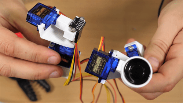
Don’t get us wrong, we have plenty of respect for [bitluni] and for the fact that he posts his failures as well as his successes, like composite video and AM radio signals from an ESP32. He used an ESP8266 in this project, which actually uses two different sensors: an ultrasonic transducer, and a small time-of-flight laser chip. Each was mounted to a two-axis scanner built from hobby servos and 3D-printed parts. The pitch and yaw axes move the sensors through a hemisphere gathering data, but unfortunately, the Wemos D1 Mini lacks the RAM to render the complete point cloud from the raw points. That’s farmed out to a WebGL page. Initial results with the ultrasonic sensor were not great, and the TOF sensor left everything to be desired too. But [bitluni] stuck with it, and got a few results that at least make it look like he’s heading in the right direction.
We expect he’ll get this sorted out and come back with some better results, but in the meantime, we applaud his willingness to post this so that we can all benefit from his pain. He might want to check out the results from this polished and pricey LIDAR scanner for inspiration.
Continue reading “Fail Of The Week: How Not To Make A 3D Scanner”
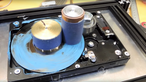
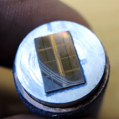 For those not into the anatomy and physiology of semiconductors, getting a look at the inside of the chip can reveal valuable information needed to reverse engineer a device, or it can just scratch the itch of curiosity. Lapping (the gentle grinding away of material) is one way to see the layers that make up the silicon die that lies beneath the epoxy. Hard drives designed to spin at 7200 rpm or more hardly seem a suitable spinning surface for a gentle lapping, but [electronupdate] just wanted the platter for its ultra-smooth, ultra-flat surface.