Easy Access Point Configuration On ESP8266

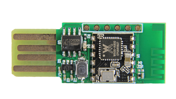
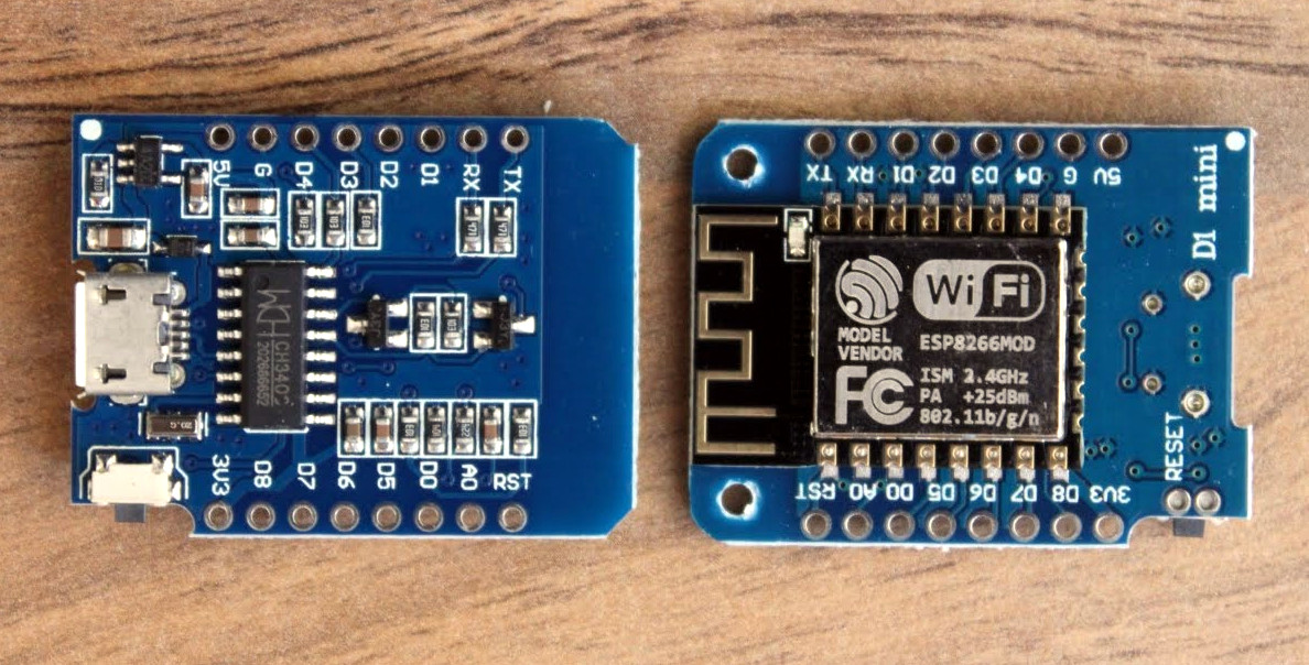
One of the biggest advantages of using the ESP8266 in your projects is how easy it is to get WiFi up and running. Just plug in the WiFi library, put the SSID and encryption key in your source code, and away you go. It authenticates with your network in seconds and you can get on with building your project. But things get a little trickier if you want to take your project someplace else, or distribute your source code to others. Quickly we learn the downside of using static variables for authentication.

While there are already a few solutions to this problem out there, [Martin Raynsford] wasn’t too thrilled with them. Usually they put the ESP8266 in Access Point mode, allow the user to connect, and then ask which network they should authenticate with. But he didn’t want his projects to require an existing network, and figured he could do just as well making a field-configurable AP.

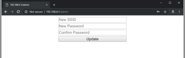
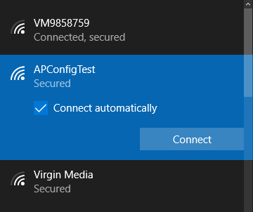
Using it is simple. Once the ESP8266 starts up it will create a new network in the form of “APConfig XXXXXX”, which should be easy enough to find from your client side device. Once connected, you can go to a simple administration page which allows you to configure a new AP name and encryption key. You even have the option to create an open AP by leaving the “Password” field blank. Once rebooted, the ESP8266 will create a new network with the defined parameters.

[Martin] has also included a “backdoor” to let anyone with physical access to the ESP8266 board create a new open AP that can be used to reconfigure the network settings. During boot up there is a brief period, indicated with specific blinks of the LED, wherein you can hit the reset button and trigger the open AP. This keeps you from getting locked out of your own project if you forget what key you gave it.

If you’re not one to go the austere route, take a look at some of the more robust solutions we’ve seen for easier end-user setup of the ESP8266.

Free ARM Cores For Xilinx FPGAs

In a surprising move, ARM has made two Cortex-M cores available for FPGA development at no cost.

In the over three decades since [Sophie Wilson] created the first ARM processor design for the Acorn Archimedes home computer, the architecture has been managed commercially such that it has become one of the most widely adopted on the planet. From tiny embedded microcontrollers in domestic appliances to super-powerful 64-bit multi-core behemoths in high-end mobile phones, it’s certain you’ll own quite a few ARM processors even if you don’t realise it. Yet none of those processors will have been made by ARM, instead the Cambridge-based company will have licenced the intellectual property of their cores to another semiconductor company who will manufacture the device around it to their specification. ARM core licences cost telephone-number sums, so unless you are a well-financed semiconductor company, until now you probably need not apply.

You will still have to shell out the dough to get your hands on a core for powerful chips like those smartphone behemoths, but if your tastes are more modest and run only to a Cortex M1 or M3 you might be in luck. For developers on Xilinx FPGAs they have extended the offer of those two processor cores at zero cost through their DesignStart Programme.

It’s free-as-in-beer rather than something that will please open-source enthusiasts, But it’s certainly a fascinating development for experimenters who want to take ARM for a spin on their own gate array. Speculation is swirling that this is a response to RISC-V, but we suspect it may be more of a partial lifting of the skirts to entice newbie developers such as students or postgraduates. If you arrive in the world of work already used to working with ARM IP at the FPGA level then you are more likely to be on their side of the fence when those telephone-number deals come up.

Thanks [Rik] for the tip!

Seeed Air602 WiFi dev board.

Tiny WiFi-Enabled ARM MCU For Tiny Projects

Ever since the ESP8266 WiFi-enabled microcontroller came on the scene, it seemed like suddenly everyone came up with WiFi-enabled projects. But the ESP8266 is not the only game in town! Reader [PuceBaboon] notified us of a new product released by Seeed Studios: the imaginatively called Air602 WiFi Development Board.

The core of this board is the tiny WinnerMicro W600 MCU, which integrates a 32-bit ARM Cortex M3 CPU, along with dual UARTs, I2C, SPI and I2S interfaces, as well as a real-time clock (RTC). Add to this hardware crypto, seven I/O pins (five broken out on the development board) and you have a very capable WiFi-enabled MCU which can be programmed using the usual ARM development tools (e.g. Keil) using the provided SDK.

The W600 module can be bought by itself, in all its diminutive 12 mm x 10 mm glory, for a mere $1.90 as of time of writing – without antenna – as noted in [PuceBaboon]’s thoughts on this MCU and the development board.

What’s The Cheapest Way To Scan Lots Of Buttons?

So you’re building a new mechanical keyboard. Or attaching a few buttons to a Raspberry Pi. Or making the biggest MIDI grid controller the world has ever know. Great! The first and most important engineering question is; how do you read all those buttons? A few buttons on a ‘Pi can probably be directly connected, one for one, to GPIO pins. A mechanical keyboard is going to require a few more pins and probably some sort of matrix scanner. But the grid controller is less clear. Maybe external I/O expanders or a even bigger matrix? Does it still need diodes at each button? To help answer these questions the folks at [openmusiclabs] generated a frankly astounding map which shows, given the number of inputs to scan and pins available, which topology makes sense and roughly how much might it cost. And to top it off they link into very readable descriptions of how each might be accomplished. The data may have been gathered in 2011 but none of the fundamentals here have changed.

How do you read this chart? The X axis is the number of free pins on your controller and the Y is the number of I/Os to scan. So looking at the yellow band across the top, if you need to scan one input it always makes the most sense to directly use a single pin (pretty intuitive, right?). Scrolling down, if you need to read 110 inputs but the micro only has eight pins free there are a couple choices, keys E and F. Checking the legend at the top E is “Parallel out shift register muxed with uC” and F is “Parallel in shift register muxed with uC“. What do those mean? Checking the table in the original post or following the link takes us to a handy descriptive page. It looks like a “parallel out shift register” refers to using a shift register to drive one side of the scan matrix, and “parallel in shift register” refers to the opposite.

Continue reading “What’s The Cheapest Way To Scan Lots Of Buttons?”

An SLA-Printed Pogo Pin Programming Jig

If you have a microcontroller to program, it can be an easy enough process to hook up a serial lead and perform the task. If however you have hundreds of microcontrollers on PCBs to program, connecting that lead multiple times becomes an impossibility. In manufacturing environments they have pogo pin jigs, an array of spring-loaded pins carrying the programming signals that line up perfectly with the appropriate pads on a PCB places on top of it.

[Conor Patrick] is working on an upgrade to the U2F Zero 2-factor authentication token, and he faces exactly this problem of needing to program a lot of boards. His pogo pin jig is very nicely executed, and he’s taken us through his design and manufacture process for it.

Starting with his PCB design in Eagle, he exported it to Fusion 360 in which he was able to create a jig to fit it. Into the jig model he placed the holes for his chosen pogo pins in the appropriate places, before printing it with an SLA 3D printer. He is particularly complementary about the pins themselves, a solder bucket design that comes from mill-Max, and was sourced via DigiKey.

The proof of the pudding is in the eating, and happily when his completed jig received its first board, everything worked as planned and the programming proceeded flawlessly. We’ve shown you other pogo pin jigs, but this one is particularly nicely executed.

Drill Jig Helps Mount WeMos D1 Mini

As far as ESP8266 boards go, the WeMos D1 Mini is a great choice if you’re looking to get started with hackerdom’s microcontroller du jour. It’s small, well supported, and can be had ridiculously cheap. Often going for as little as $3 USD each, we buy the things in bulk just to have spares on hand. But that’s not to say it’s a perfect board. For one, it lacks the customary mounting holes which would allow you to better integrate it into finished products.

This minor annoyance was enough to spring [Martin Raynsford] into action. He noticed there was some open area on the D1 Mini’s PCB where it seemed he could drill through to add his own mount points, but of course popping holes in a modern PCB can be risky business. There’s not a lot of wiggle room between success and heartbreak, and it’s not like the diminutive D1 Mini is that easy to hold down to begin with. So he designed a laser-cut jig to allow him to rapidly add mounting holes to his D1 Mini’s assembly line style.

For those who might be skeptical, [Martin] reports he’s seen no adverse effects from drilling through the board, though does admit it’s possible the close proximity of the metal screw heads to the ESP8266’s antenna may have a detrimental effect. That said, he’s tested them in his projects out to 25 m (82 feet) with no obvious problems. He’s using a 2 mm drill bit to make his hole, and M2 x 6 mm machine screws to hold the boards down.

The jig design is released as a SVG and DXF for anyone with a laser cutter to replicate, but it shouldn’t be too difficult to extrude those designs in the Z dimension for hackers who haven’t yet jumped on the subtractive manufacturing bandwagon.

When a project makes the leap from prototype to in-house production, designing and building jigs become an essential skill. From flashing firmware to doing final checkout, the time and effort spent building a jig early on will pay for itself quickly in production.

Trials And Tribulations In Sending Data With Wires

When working on a project that needs to send data from place to place the distances involved often dictate the method of sending. Are the two chunks of the system on one PCB? A “vanilla” communication protocol like i2c or SPI is probably fine unless there are more exotic requirements. Are the two components mechanically separated? Do they move around? Do they need to be far apart? Reconfigurable? A trendy answer might be to add Bluetooth Low Energy or WiFi to everything but that obviously comes with a set of costs and drawbacks. What about just using really long wires? [Pat] needed to connect six boards to a central node over distances of several feet and learned a few tricks in the process.

When connecting two nodes together via wires it seems like choosing a protocol and plugging everything in is all that’s required, right? [Pat]’s first set of learnings is about the problems that happen when you try that. It turns out that “long wire” is another way to spell “antenna”, and if you happen to be unlucky enough to catch a passing wave that particular property can fry pins on your micro.

Plus it turns out wires have resistance proportional to their length (who would have though!) so those sharp square clock signals turn into gently rolling hills. Even getting to the point where those rolling hills travel between the two devices requires driving drive the lines harder than the average micro can manage. The solution? A differential pair. Check out the post to learn about one way to do that.

It looks like [Pat] needed to add USB to this witches brew and ended up choosing a pretty strange part from FTDI, the Vinculum II. The VNC2 seemed like a great choice with a rich set of peripherals and two configurable USB Host/Peripheral controllers but it turned out to be a nightmare for development. [Pat]’s writeup of the related troubles is a fun and familiar read. The workaround for an incredible set of undocumented bad behaviors in the SPI peripheral was to add a thick layer of reliability related messaging on top of the physical communication layer. Check out the state machine for a taste, and the original post for a detailed description.