Rural Hacker De-Crufts And Rebuilds Hydroelectric Generator

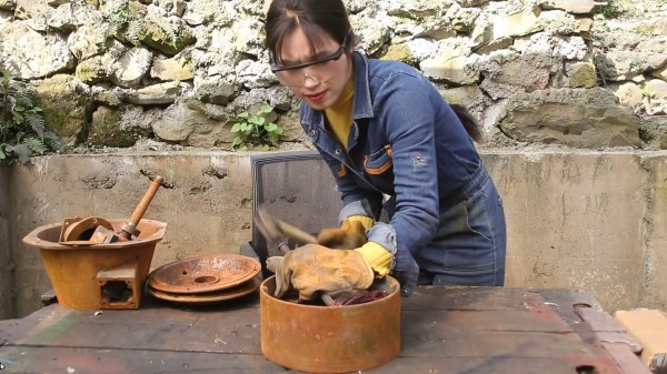
YouTuber [Linguoer] has a knack, and it’s one that we don’t often see on the pages of Hackaday: rewinding and rebuilding dilapidated motors and generators. In the video below, you’ll see [Lin] take a hydroelectric turbine and generator that looks like it’s been sitting at the bottom of a lake, and turn it into a working unit, all while wearing her trademark blue and yellow denim jumpsuit.

Where as most makers would have used a MIG or TIG welder, [Linguoer] uses a simple (probably A/C) stick welder. Generator windings are calculated and wound by hand, and the carcass of what used to be the generator is sandblasted out in the open. Missing parts are fabricated from scratch using nothing more than an angle grinder. “Simple” is the order of the day.

[Linguoer] often refers to herself as “Village Girl”. Whatever specialty tools she uses, they are elementary. And whatever methods she uses, they are manual. You will get the idea very quickly that [Linguoer] isn’t just a person with a skill, but a person with a passion for getting things done no matter the circumstances. [Linguoer] is a hacker if there ever was one!

If hydroelectric hacks spin your pelton wheel, give this Impressive Off-Grid Hydroelectric Plant a whirl.

Continue reading “Rural Hacker De-Crufts And Rebuilds Hydroelectric Generator”

Reverse Engineering Your Own Bluetooth Audio Module

There was a time when we would start our electronic projects with integrated circuits and other components, mounted on stripboard, or maybe on a custom PCB. This is still the case for many devices, but it has become increasingly common for an inexpensive ready-built module to be treated as a component where once it would have been a project in its own right. We’re pleased then to see the work of [ElectroBoy], who has combined something of both approaches by reverse engineering the pinout of a Chinese Bluetooth audio chip with minimal datasheet, and making his own take on an off-the-shelf Bluetooth audio module.

The JL_AC6939B comes in an SOIC16 package and requires a minimum number of components. The PCB is therefore a relatively simple proposition and indeed he’s fitted all parts and traces on one side with the other being a copper ground plane. It’s dangerous to assume that’s all there is to a board like this one though, because many an engineer has come unstuck trying to design a PCB antenna. We’d hazard a guess that the antenna here is simply a wavy PCB line rather than an antenna with a known impedance and bandwidth, at the very least it looks to have much thicker traces than the one it’s copying.

It’s possible that it’s not really worth the effort of making a module that can be bought for relative pennies ready-made, but to dismiss it is to miss the point. We make things because we can, and not merely because we should.

The BGA chip in question flipped onto a piecce of breadboard, all its pins broken out with magnet wire.

Heroic Efforts Give Smallest ARM MCU A Breakout, Open Debugger

In today’s episode of Diminutive Device Technology Overview, [Sprite_TM] is at it again – this time conquering the HC32L110. A few weeks ago, we have highlighted the small ARM Cortex M0+ microcontroller, which is outstanding because of its exceptionally small size. We also pointed out a few hurdles, among them – hard-to-approach SDK and documentation, and difficulties making and assembling a PCB for such a small BGA. Today, we witness how [Sprite_TM] bulldozed through all of these hurdles for all of us, and added a few pictures to our collective “outrageous soldering” galleries while at it.

First, he figured out an example layout for this MCU that’s achievable for us even on a cheapest 2-layer board from JLCPCB, keeping distances within the generic tolerance standards by snubbing out a few pins. As a result, we only lose access to four GPIOs – those will have to be kept as inputs, so that nothing burns out. However, that’s the kind of tradeoff we are okay making if it helps us keep our PCB small and lightweight for projects where these factors matter. After receiving the resulting board, he also recorded a short tutorial on soldering such packages at home with a mere hot air gun and a few bare necessities like flux and tweezers – embedded below.

It doesn’t end there, however, as he decided to work around the GPIO fanout limitation in a non-intended way. Evidently, [Sprite_TM] decided to have some fun, taking a piece of regular 0.1″ spacing protoboard and deadbugging the chip with magnet wire, much to our amusement. The resulting contraption, pictured above, worked – and this is ever something you’d like to be able to achieve yourself in times of dire need, whether you make something work or simply to be entertained by making use of a cursed mounting technique, there’s an one-hour-long livestream recording of how this magnet wire contraption came to be. And, of course, that wasn’t the last thing to be shared.

Continue reading “Heroic Efforts Give Smallest ARM MCU A Breakout, Open Debugger”

3D Printing Snap Fit Joints

Owning a 3D printer seems to progress through stages. You start printing simple shapes. Then you get serious about calibration and quality. Eventually, you move to trying to design and build practical things. To get practical, you often need to join parts together and that requires glue, fasteners, threaded inserts, and plastic welding. However, you can also make parts that fit together using friction and the springiness of plastic. For example, [Lucas Carolo] recently had a look at 3D printing snap-fit joints. These are commonly seen on the end of straps so that you can connect two ends together.

Of course, you can use them anywhere you need a secure connection. However, you might want to consider that since the jaws compress, there will be repeated stress on the part, so it might not be a good choice for items that you will frequently snap together. Also, brittle plastic such as PLA might not be the best choice of materials. There are several different kinds of joints. The cantilever version has a hook that bends into place and, as mentioned earlier, is common on luggage or backpack straps. The post offers tips on how to design a durable hook. In particular, the orientation of the hook during printing is critical because of the stress involved.

Another type of snap-fit joint is the kind you find on many snap electronic enclosures or things like pen caps. In these joints, a large bump (a boss) fits into a similar groove on the other part. The post has a little less information on these but does mention that you should form the bosses with a chamfer. If you want more details, the post links to a great guide and an enclosure tutorial that you should check out.

We’ve covered this topic before and have some other guides to check out. We’ve also seen some pretty innovative connecting methods.

Class A Amplifiers, Virtually

If you didn’t know better, you might think the phrase “class A amplifier” was a marketing term to help sell amplifiers. But it is, of course, actually a technical description of an amplifier that doesn’t distort the input waveform because it doesn’t depend on multiple elements to handle different areas of the input waveform. Want to know more? [FesZ] has a new video covering the basics of class A amplifiers including some great simulations. You can see the video below.

A class A amplifier uses a transistor that is always biased on. It never saturates or switches off. This is good for linearity, but not always the best for efficiency so there are other classes of amplifiers, too. However, for many applications, class A is the most common configuration.

There are a number of trade-offs involved with each type of amplifier and [FesZ] covers them in detail. But the real interesting part is the simulations in Spice. Sure, you can build the circuits and look at everything with a meter or scope, but using Spice is much handier.

There is a second video upcoming. We hope he covers other amplifier types too, as you really do want to understand the differences when you need to design something. If you want more Spice stuff, check out some of our previous posts. If for some reason, you don’t like LTSpice, there’s always Micro-Cap 12.

Continue reading “Class A Amplifiers, Virtually”

Top side of the VL670 breakout board, with two USB connectors and the VL670 chip in the center.

A Chip To Bridge The USB 2 – USB 3 Divide

On Twitter, [whitequark] hasĀ  found and highlighted an intriguing design – a breakout board for the VL670, accompanied by an extensive yet very easy to digest write-up about its usefulness and inner workings. The VL670 is a chip that addresses a surprising problem – converting USB 2.0 signals into USB 3.0.

If you have a USB 2.0 device and a host with only USB 3.0 signals available, this chip is for you. It might be puzzling – why is this even needed? It’s about the little-known dark secret of USB3, that anyone can deduce if they ever have to deal with a 9-pin USB 3.0 connector where one of the three differential pairs doesn’t quite make contact.

When you see a blue “3.0” port, it’s actually USB 2 and USB 3 — two separate interfaces joined into a single connector. USB 3 uses two single-directional differential pairs, akin to PCI-E, whereas USB 2 uses a single bidirectional one, and the two interfaces on a blue connector operate basically independently of each other. There’s many implications to this that are counterintuitive if you simply take “USB 3.0” for “faster backwards-compatible USB”, and they have painful consequences.

For instance, USB 3 hub ICs have two separate hub entities inside – one for USB 3 and one for USB 2. Even if you have a USB 3 hub plugged into a USB 3 port, multiple USB 2 devices plugged into it still cannot break through the USB 2 uplink limit of 480 MBps. If you ever thought that a faster hub with a faster uplink would fix your USB 2 device speed problems – USB-IF engineers, apparently, thought differently; and you might have to find a workaround for your “many cheap SDRs and Pi 4 in a box” setup. Continue reading “A Chip To Bridge The USB 2 – USB 3 Divide”

The teeny tiny MCU mentioned in the article, merely a blimp on a giant devboard

New Part Day: Smallest ARM MCU Uproots Competition, Needs Research

We’ve been contacted by [Cedric], telling us about the smallest ARM MCU he’s ever seen – Huada HC32L110. For those of us into miniature products, this Cortex-M0+ package packs a punch (PDF datasheet), with low-power, high capabilities and rich peripherals packed into an 1.6mm x 1.4mm piece of solderable silicon.

This is matchstick head scale computing, with way more power than we previously could access at such a scale, waiting to be wrangled. Compared to an 8-bit ATTiny20 also available in WLCSP package, this is a notable increase in specs, with a way more powerful CPU, 16 times as much RAM and 8-16 times the flash! Not to mention that it’s $1 a piece in QTY1, which is about what an ATTiny20 goes for. Being a 0.35mm pitch 16-pin BGA, your typical board house might not be quite happy with you, but once you get a board fabbed and delivered from a fab worth their salt, a bit of stenciling and reflow will get you to a devboard in no time.

Drawbacks? No English datasheet or Arduino port, and the 67-page PDF we found doesn’t have some things like register mappings. LILYGO promised that they will start selling the devboards soon, but we’re sure it wouldn’t be hard for us to develop our own. From there, we’d hope for an ESP8266-like effect – missing information pieced together, translated and made accessible, bit by bit.

When it comes to soldering such small packages, we highly recommend reflow. However, if you decide to go the magnet wire route, we wouldn’t dare object – just make sure to send us pictures. After all, seems like miniature microcontrollers like ATTiny20 are attractive enough of a proposition that people will pick the craziest route possible just to play with one. They say, the madness of the brave is the wisdom of life.

We thank [Cedric] for sharing this with us!