Opening Up ASIC Design

The odds are that if you’ve heard about application-specific integrated circuits (ASICs) at all, it’s in the context of cryptocurrency mining. For some currencies, the only way to efficiently mine them anymore is to build computers so single-purposed they can’t do anything else. But an ASIC is a handy tool to develop for plenty of embedded applications where efficiency is a key design goal. Building integrated circuits isn’t particularly straightforward or open, though, so you’ll need some tools to develop them such as OpenRAM.

Designing the working memory of a purpose-built computing system is a surprisingly complex task which OpenRAM seeks to demystify a bit. Built in Python, it can help a designer handle routing models, power modeling, timing, and plenty of other considerations when building static RAM modules within integrated circuits. Other tools for taking care of this step of IC design are proprietary, so this is one step on the way to a completely open toolchain that anyone can use to start building their own ASIC.

This tool is relatively new and while we mentioned it briefly in an article back in February, it’s worth taking a look at for anyone who needs more than something like an FPGA might offer and who also wants to use an open-source tool. Be sure to take a look at the project’s GitHub page for more detailed information as well. There are open-source toolchains if you plan on sticking with your FPGA of choice, though.

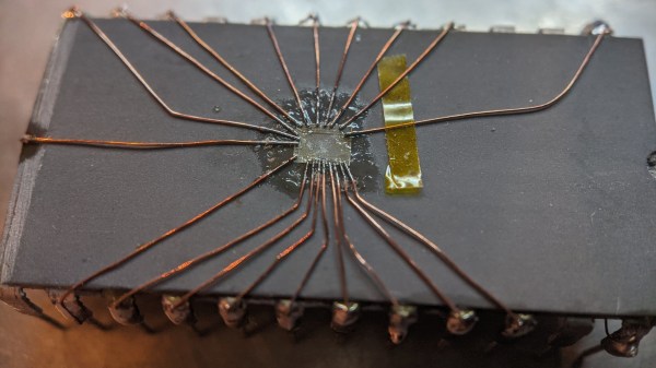
The decapped chip on top of some other DIP IC, with magnet wire soldered to the die, other ends of the magnet wire soldered to pins of the "body donor" DIP IC.

Factory Defect IC Revived With Sandpaper And Microsoldering

We might be amidst a chip shortage, but if you enjoy reverse-engineering, there’s never a shortage of intriguing old chips to dig into – and the 2513N 5×7 character ROM is one such chip. Amidst a long thread probing a few of these (Twitter, ThreadReader link), [TubeTime] has realized that two address lines were shorted inside of the package. A Twitter dopamine-fueled quest for truth has led him to try his hand at making the chip work anyway. Trying to clear the short with an external PSU led to a bond wire popping instead, as evidenced by the ESD diode connection disappearing.

A dozen minutes of sandpaper work resulted in the bare die exposed, making quick work of the bond wires as a side effect. Apparently, having the bond pads a bit too close has resulted in a factory defect where two of the pads merged together. No wonder the PSU wouldn’t take that on! Some X-acto work later, the short was cleared. But without the bond wires, how would [TubeTime] connect to it? This is where the work pictured comes in. Soldering to the remains of the bond wires has proven to be fruitful, reviving the chip enough to continue investigating, even if, it appears, it was never functional to begin with. The thread continued on with comparing ROMs from a few different chips [TubeTime] had on hand and inferences on what could’ve happened that led to this IC going out in the wild.

Such soldering experiments are always fun to try and pull off! We rarely see soldering on such a small scale, as thankfully, it’s not always needed, but it’s a joy to witness when someone does IC or PCB microsurgery to fix factory defects that render our devices inoperable before they were even shipped. Each time that a fellow hacker dares to grind the IC epoxy layers down and save a game console or an unidentified complex board, the world gets a little brighter. And if you aren’t forced to do it for repair reasons, you can always try it in an attempt to build the smallest NES in existence!

Continue reading “Factory Defect IC Revived With Sandpaper And Microsoldering”

Garage Semiconductor Fab Gets Reactive-Ion Etching Upgrade

It’s a problem that few of us will likely ever face: once you’ve built your first homemade integrated circuit, what do you do next? If you’re [Sam Zeloof], the answer is clear: build better integrated circuits.

At least that’s [Sam]’s plan, which his new reactive-ion etching setup aims to make possible. While his Z1 dual differential amplifier chip was a huge success, the photolithography process he used to create the chip had its limitations. The chemical etching process he used is a bit fussy, and prone to undercutting of the mask if the etchant seeps underneath it. As its name implies, RIE uses a plasma of highly reactive ions to do the etching instead, resulting in finer details and opening the door to using more advanced materials.

[Sam]’s RIE rig looks like a plumber’s stainless steel nightmare, in the middle of which sits a vacuum chamber for the wafer to be etched. After evacuating the air, a small amount of fluorinated gas — either carbon tetrafluoride or the always entertaining sulfur hexafluoride — is added to the chamber. A high-voltage feedthrough provides the RF energy needed to create a plasma, which knocks fluorine ions out of the process gas. The negatively charged and extremely reactive fluorine ions are attracted to the wafer, where they attack and etch away the surfaces that aren’t protected by a photoresist layer.

It all sounds simple enough, but the video below reveals the complexity. There are a lot of details, like correctly measuring vacuum, avoiding electrocution, keeping the vacuum pump oil from exploding, and dealing with toxic waste products. Hats off to [Sam’s dad] for pitching in to safely pipe the exhaust gases through the garage door. This ties with [Huygens Optics]’s latest endeavor for the “coolest things to do with fluorine” award.

Continue reading “Garage Semiconductor Fab Gets Reactive-Ion Etching Upgrade”

[Ken Shirriff] Picks Apart Mystery Chip From Twitter Photo

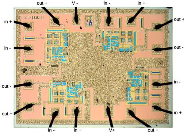
It’s no secret that the work of [Ken Shirriff] graces the front pages of Hackaday quite frequently. He’s back again, this time reverse engineering a comparator chip from a photo on Twitter. The mysterious chip was decapped, photographed under a microscope, and subsequently posted on the internet with an open call to figure out what it did.

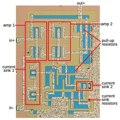
[Ken] stepped up, and at first glance, it was obvious that most of the chip is unused, and there appeared to be four copies of the same circuit. After identifying resistors and the different transistor types, [Ken] found differential pairs.

Differential pairs form the heart of most op-amps, and by chaining them together, you can get a strong enough signal to treat it as a logic signal. Based on the design and materials, [Ken] estimates the chip is from the 1970s. Given that it appears to be ECL (Emitter-Coupled Logic), it could just be four comparators. But there are still a few things that don’t add up as two comparators have additional inverted outputs. Searching the part number offered few if any clues, so this will remain somewhat a mystery.

We’ve covered [Ken’s] incredible chip sleuthing before here, such as the Sharp EL-8 from 1969.

Decapping Components Hack Chat With John McMaster

Join us on Wednesday, March 10 at noon Pacific for the Decapping Components Hack Chat with John McMaster!

We treat them like black boxes, which they oftentimes are, but what lies beneath the inscrutable packages of electronic components is another world that begs exploration. But the sensitive and fragile silicon guts of these devices can be hard to get to, requiring destructive methods that, in the hands of a novice, more often than not lead to the demise of the good stuff inside.

To help us sort through the process of getting inside components, John McMaster will stop by the Hack Chat. You’ll probably recognize John’s work from Twitter and YouTube, or perhaps from his SiliconPr0n.org website, home to beauty shots of some of the chips he has decapped. John is also big in the reverse engineering community, organizing the Mountain View Reverse Engineering meetup, a group that meets regularly to discuss the secret world of components. Join us as we talk to John about some of the methods and materials used to get a look inside this world.

join-hack-chatOur Hack Chats are live community events in the Hackaday.io Hack Chat group messaging. This week we’ll be sitting down on Wednesday, March 10 at 12:00 PM Pacific time. If time zones have you tied up, we have a handy time zone converter.

Click that speech bubble to the right, and you’ll be taken directly to the Hack Chat group on Hackaday.io. You don’t have to wait until Wednesday; join whenever you want and you can see what the community is talking about.
Continue reading “Decapping Components Hack Chat With John McMaster”

Hackaday Links Column Banner

Hackaday Links: December 20, 2020

If development platforms were people, Google would be one of the most prolific serial killers in history. Android Things, Google’s attempt at an OS for IoT devices, will officially start shutting down on January 5, 2021, and the plug will be pulled for good a year later. Android Things, which was basically a stripped-down version of the popular phone operating system, had promise, especially considering that Google was pitching it as a secure alternative in the IoT space, where security is often an afterthought. We haven’t exactly seen a lot of projects using Android Things, so the loss is probably not huge, but the list of projects snuffed by Google and the number of developers and users left high and dry by these changes continues to grow. Continue reading “Hackaday Links: December 20, 2020”

Why Some Chips Have Inconvenient Pinouts

If you’ve ever handled a chip with a really strange or highly inconvenient pinout and suspected that the reason had something to do with the inner workings, you may be interested to see [electronupdate]’s analysis of why the 4017 Decade Counter IC has such a weirdly nonintuitive pinout. It peeks into an IC design dating from the 1970s to see an example of the kind of design issues that can affect physical layout.

Inside the 4017. Want to make sense of how lines and shapes on a silicon wafer make an IC work? With the right teachers, it’s simple.

In the case of the 4017, once decapped and the inner workings exposed, things became more clear. Inside the chip are a bunch of flip-flops and NAND gates, laid out in a single layer. Some of the outputs (outputs 5 and 1 for example, physically on pins 1 and 2 respectively) share the same flip-flop.

The original design placed the elements in a way that made the most logical sense for routing and layout, which resulted in nice and tidy inner workings but an apparently illogical pinout. A lot of this is probably feeling familiar to anyone who has designed and routed a single-layer PCB, where being limited to one layer makes it important to get the most connections as directly near one another as possible.

Chip design has of course come a long way since the 70s, but there is forever some level of trade-off to be made between outward tidiness and inner design harmony. The next time you’re looking at a part with an apparently illogical pinout, there’s a fair chance it makes far more sense on the inside.

If any of you are interested in decapping ICs yourselves to see what’s inside, we saw that it’s possible with commonly available chemicals, not just nasty ones.

Continue reading “Why Some Chips Have Inconvenient Pinouts”