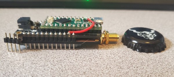
In a world of always-connected devices and 24/7 access to email and various social media and messaging platforms, it’s sometimes a good idea to take a step away from the hustle and bustle for peace of mind. But not too big of a step. After all, we sometimes need some limited contact with other humans, so that’s what [EverestX] set out to do with his modern, pocket-sized communication device based on pager technology from days of yore.
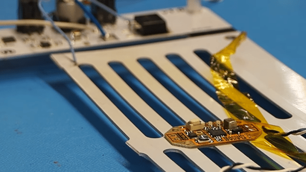
The device uses the POCSAG communications protocol, a current standard for pager communications that allows for an SMS-like experience for those still who still need (or want) to use pagers. [EverestX] was able to adapt some preexisting code and port it to an Atmel 32u4 microcontroller. With a custom PCB, small battery, an antenna, and some incredibly refined soldering skills, he was able to put together this build with an incredibly small footprint, slightly larger than a bottle cap.
Once added to a custom case, [EverestX] has an excellent platform for sending pager messages to all of his friends and can avoid any dreaded voice conversations. Pager hacks have been a favorite around these parts for years, and are still a viable option for modern communications needs despite also being a nostalgic relic of decades past. As an added bonus, the 32u4 microcontroller has some interesting non-pager features that you might want to check out as well.
Thanks to [ch0l0man] for the tip!

 The software in question is