A Desk Calendar With A Difference

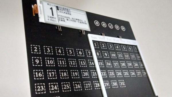
With the office computer revolution now many decades old, many of the items that once stood on a typical desk are now part of history. The typewriter, the Rolodex, and the desk calendar have all been subsumed by computers and mobile phones. This electronic desk calendar is perhaps an exception, created as a promotional device for the RT-Thread IoT OS. It features an interesting take on a perpetual calendar, with an array of days spanned by a sliding frame such that any month’s days of the week can be depicted. The days are touch buttons, and can be used to bring up the information on an e-ink display.

Behind it all is a WinnerMicro W600 WiFi-enabled system-on-chip, that runs the aforementioned RT-Thread IoT OS. This OS is a bit of a mystery, according to its Wikipedia page it’s an open-source project from China with ten years of development behind it, but this appears to be the first time we’ve seen it here at Hackaday. Anyone using it?

We like this project though, for its perpetual calendar, and for its re-imagining of a bygone desk accoutrement with an e-ink display to conserve battery. It’s not the first e-ink calendar we’ve seen, this previous one used a Raspberry Pi.

Making PCBs The Easy Way

Building a PCB at home can be fraught. If you’re etching, there are chemicals and the nuances of toner transfer. If you’re milling, getting the surface height just right, and not breaking those pointy little v-cutters is always a challenge. [Robin] has tips for both of these cases, and solves a lot of the common hassles by using a milling machine.

Whether he’s scraping away etch resist or entire copper isolation lines, [Robin] uses a non-spinning scratching tool instead of a v-bit: they’re more robust and cut every bit as well. He’s got tips for using FlatCam and KiCAD to make scratched-out traces. His registration system allows him to get double-sided boards with a minimum of hassle. And as a bonus, he’s doing some experimentation with embedding SMT parts inside the boards as well. Be sure that you check out his whole guide, or just watch the video embedded below.

We’re pretty sure you’ll pick up a trick or two, and maybe you’ll be convinced to bite the bullet and invest in a nice mill. If you’d like a more traditional take on PCB milling, try out our own [Adil Malik]’s guide.

Continue reading “Making PCBs The Easy Way”

Live Map Of London Tube Created In PCB And Lights

If you’re a frequent traveler on a public transit system, it can be helpful to know when the trains or buses are arriving and if there are any delays. We might reach for a tablet to mount on the wall, but that relies on keeping the OS, the software, and its library dependancies up to date. For true reliability you’ll need to build directly in hardware, which is exactly what this map of the London tube system uses.

The base map is printed directly on PCB, with LEDs along each of the major routes to indicate the current location of the trains. A few small chips handle the WiFi connection — it appears to our eye to be an ESP8266 — and pulling the information about the trains from the London Underground API (it would be virtually impossible to build everything for this project in hardware). The hardware can be easily reprogrammed, and with the PCB layout this could be adapted for other public transit fairly easily.

Even apart from the philosophical differences on design between hardware and software approaches, we still appreciate the aesthetic of LEDs on PCB. In fact, we’ve seen a whole host of artwork on PCBs ever since the price came down dramatically in the past two decades.

Thanks to [Al] for the tip!

Tidy Laser Cut Packaging For PCBs With KiCAD

A laser cutter is a useful tool to have in any workshop. While many hackers use them for their cutting abilities, it’s important to remember that they can be great as engravers, too. [Wrickert] was well aware of this when he set his to work, producing attractive packaging for his Tindie orders.

[Wrickert] sells a variety of small PCB-based devices on Tindie, and it’s nice to have something to package them up with, rather than just sending a bare board. To do this quickly and effectively, KiCAD is used to help generate the packaging from the original PCB geometry itself. The board outlines are exported as an SVG file, reopened in KiCAD, and then used to create the required cardboard parts. The laser can then also be used to engrave the cardboard too.

It’s a tidy packaging solution that requires no messy inks or printers, and can be designed in the same software as the device itself. We’ve covered this area before, talking about what it takes to go from a home project to a saleable kit. If you’re in the game, you might find [Wrickert]’s hack to be just the ticket!

Hinge Brings New Meaning To Flexible PCB

It is not a secret that flexible PC boards can bend. But despite the substrate’s flexibility, you can’t really fold them completely over. That bothered [Carl] so he developed a hinge design so that he can fold a board completely in half. You can watch a video showing an example, FlexBox, below.

Normal boards can fold over, but the copper traces can’t tolerate a very tight bend radius. [Carl’s] trick is to make the folding part have no traces at all. Only a small bridge carries traces between the two halves and it is allowed to bend almost like an interconnecting cable.

Continue reading “Hinge Brings New Meaning To Flexible PCB”

How CERN Made High Quality Electronics In The 1970s

We’re suckers for some retro electronics here at Hackaday, so we were fascinated when Daniel Valuch wrote to us with some pictures of his findings in his CERN lab’s archive. He works on Linear Accelerator 3, which has had an extended downtime after many decades of continuous operation, for major upgrades and overhauls. Part of the upgrade involves the removal of electronic assemblies dating back as far as the 1970s, and he’s shared his fascination with them as he trawls through dusty filing cabinets in the lab basement.

What it reveals is a world before the CAD and microcontrollers we know, instead here are circuits using the electronic building blocks of logic gates, discretes, and op-amps. PCBs are laid out not with the KiCad that CERN are famous in our community for today, but on acetate, with transfers and tape. A ground plane is even hand-carved from a red sheet. Oddly though it isn’t a world without CNC, because in the pouch with a design from 1974 is a roll of punched paper tape. If you have ever pondered the “Numerical” in “Computer Numerical Control”, here are the numbers in physical form.

For those of us who were trained in this type of electronic design, the convenience of a PCB CAD package and a professionally-made PCB at the click of a mouse is nothing short of miraculous. But seeing personally laid boards of this quality reminds us that seeing the hand of the designer in them is something few engineers today (with the possible exception of Boldport) manage to recreate.

Soon… Inkjet Your Circuit Boards

Printed circuit board fabrication — especially in basements and garages — have been transformed by the computer revolution. Before that, people would use a permanent marker or little decals to layout circuit boards prior to etching. Sometimes, they’d do it on film and use a photo process, but they did make decals that you applied directly to the board to resist the etch. Now a team from Georgia Tech, University of Tokyo, Carnegie Mellon, and the University of Nebraska has brought things full circle. Their process inkjet prints silver traces on a substrate that they can then transfer to a circuit board — no etching required.

They start with a standard Epson inkjet with cartridges that have silver-bearing ink. The patterns print on a transfer paper that ensures the particles fuse so there’s no sintering step required to make sure the traces are all conductive. A sticky backing is applied and peels the pattern off the transfer paper. You can see more in the video below.

Continue reading “Soon… Inkjet Your Circuit Boards”