Stuck Designing Two-Layer PCBs? Give Four Layers A Try!

Many readers are certainly familiar with the process for home-etching of PCBs: it’s considered very straightforward, if a little involved, today. This was not the case in my youth, when I first acquired an interest in electronics. At that time, etching even single-sided boards was for “advanced” hobbyists. By the time I started etching my own PCBs, the advanced hobbyists were on to double-sided home-etched boards — the only type not pictured above, because I couldn’t find the one successful example I ever created. I later saw the rise of “bare bones” fabricated PCBs: professionally made fixed size boards with plated-through holes, but no soldermask or silkscreen. Eventually, this gave way to the aggregating PCB services we have now with full two-layer boards, complete with soldermask and silkscreen.

Today, the “advanced” hobbyist may be using four-layer boards, although the four-layer adoption rate is still relatively low – OSH Park produces around 90% two-layer and 10% four-layer, for instance. I think this will inevitably increase, as has been the case with all the previous technologies: the advanced eventually becomes the mainstream. Each of the previous shifts has brought easier design and construction as well as improved performance, and the same will be true as four layers becomes more commonplace.

So, let’s take a look at designing four-layer PCBs. If you’ve never considered one for any of your designs, you may be pleasantly surprised at what little extra cost is involved for all the benefits you gain. Continue reading “Stuck Designing Two-Layer PCBs? Give Four Layers A Try!”

Imitating Art In Life With A Reverse-Engineered Tattoo

In general, tattoo artists are not electrical engineers. That’s fine; the world needs both professions. But when you need a circuit designed, you’re better off turning to an EE rather than a tattoo artist. And you certainly don’t want an EE doing your new ink. Disaster lies that way.

Surprisingly, [Missa]’s tattoo of a heart-shaped circuit turned out at least to be plausible design, even if it’s not clear what it’s supposed to do. So her friend [Jeremy Elson] took up the challenge to create a circuit that looked like the tattoo while actually doing something useful. He had to work around the results of tattoo artistic license, like sending traces off to the board’s edge and stranding surface-mount components without any traces. The artist had rendered an 8-pin DIP device, albeit somewhat proportionally challenged, so [Jeremy] went with an ATtiny85, threw on a couple of SMD resistors and a cap, and placed two LEDs for the necessary blinkenlights. Most of the SMDs are fed from traces on the back of the board that resurface through vias, and a small coin cell hidden on the back powers it. One LED blinks “Happy Birthday [Missa]” in Morse, while the other blinks prime numbers from 2 to 23 – we’ll assume this means it was [Missa]’s 23rd birthday.

There’s a surprising amount of crossover between the worlds of electronics and tattooing. We’ve featured functional temporary tattoo circuits, prison-expedient tattoo guns, and even a CNC tattoo machine.

Continue reading “Imitating Art In Life With A Reverse-Engineered Tattoo”

Create Green, Soldermasked PCBs With Fritzing

Even though you can easily order a PCB from any one of a dozen board houses and have it on your desk in a few weeks, there’s still a need for home-made circuit boards. If it’s because you have very special or strange requirements, you want to save money, or you need to suffer for your art, you can make printed circuit boards at home. You can even apply soldermask. It’s easy, and [Renzo] is here to show you how.

The beginnings of this tutorial cover well-tread territory such as building a CNC router, laying out a circuit, and cutting a piece of single-sided, copper clad board. If you stopped right there, after milling traces into a board, you would have a functioning circuit. But it wouldn’t look good; a piece of copper does not a PCB make, and you need soldermask. That’s where the real work comes in.

Applying the soldermask meant there needed to be places without soldermask, mostly the vias and through-holes. For this, [Renzo] pulled the copper pad layer out of Fritzing, printed it on a transparency sheet, and finally applied the UV-curing soldermask. This came as a kit, and right now, you can get 10 ml of green, red, blue, yellow, and black UV-curing soldermask, and a UV flashlight for ten dollars on the usual Internet shops. This soldermask was lathered on, rolled out, and exposed with the UV flashlight. After a quick wash in acetone, the result is a perfect PCB.

CNC Your Own PCB With This Tutorial

It is getting so easy to order a finished printed circuit board that it is tough to justify building your own. But sometimes you really need a board right now. Or maybe you need a lot of fast iterations so you can’t wait for the postal service. [Thomas Sanladerer] shows how he makes PCBs with a CNC machine and has a lot of good advice in the video below.

He starts with Eagle, although, you could use any creation package. He shows what parameters he changes to make sure the traces don’t get eaten away and how to do the CAM job to get the files required to make the boards. If you don’t use Eagle, you’ll need to infer how to do similar changes and get the same kind of output.

We’ve only heard a few people pronounce Gerber (as in Gerber file) with a soft G sound, but we still knew what he meant. We have the same problem with GIF files. However, once you have Gebers, you can join the video’s workflow about 5 minutes in.

At that point, he uses FlatCAM to convert the Gerbers to a single G-code file that integrates the paths and drill files. There were a few tricks he used to make sure all the tracks are picked up. Other tricks include leveling a spoil board by just milling it down and mounting different size bits. He also has ideas on aligning the Z axis.

Continue reading “CNC Your Own PCB With This Tutorial”

Reverse Engineering Keeps Keck Telescopes On Track

Perched atop a dormant volcano far above the roiling tropical air of the Big Island of Hawai’i sit two of the largest optical telescopes in the world. Each 10-meter main mirror is but a single part of a magnificent machine weighing in at some 400 tons that needs to be positioned with incredible precision. Keeping Keck 1 and Keck 2 in peak operating condition is the job of a team of engineers and scientists, so when the servo amplifiers running the twelve motors that move each scope started to show their age, [Andrew] bit the bullet and rebuilt the obsolete boards from scratch.

The Keck telescopes were built over three decades ago, and many of the parts, including the problematic servo amps, are no longer made. Accumulated wear and tear from constant use and repeated repairs had taken their toll on the boards, from overheated components to lifted solder pads. With only some barely legible schematics of the original amplifiers to go by, [Andrew] reverse engineered new amps. Some substitutions for obsolete components were needed, the PCB design was updated to support SMD parts, and higher-quality components were specified, but the end result is essentially new amplifiers that are plug-in replacements for the original units. This should keep the telescopes on track for decades to come.

Not to sound jealous, but it seems like [Andrew] has a great gig. He’s shared a couple of his Keck adventures before, like the time a failed LED blinded the telescope. He’s also had a few more down-to-earth hacks, like fixing a dodgy LCD monitor and making spooky blinkeneyes for Halloween.

Hackaday Links Column Banner

Hackaday Links: February 24, 2019

Back To The Future Part II, released in 1989, told us the far-off future of 2015 would have flying cars, drones working for national newspapers, and self-lacing sneakers. Our best hope for flying cars is Uber, and that’s going to be hilarious when it fails. (Note to Uber: buy KSMO, Santa Monica airport, as an air taxi hub because that’s the most hilarious of all possible realities.) National newspapers — heck, even newspapers — don’t exist anymore. Self-lacing sneakers? Nike’s self-lacing sneakers brick themselves with a firmware update. Don’t worry, it’s only the left shoe.

HackSpace magazine Vol. 16 is out, and there’s a few pages dedicated to Tindie from the person who runs it, our fabulous [Jasmine]. There’s some good tips in here for Tindie sellers — especially shipping — and a good introduction to what Tindie actually is. The three-second elevator pitch of, ‘Etsy but for DIY electronics’ is not in the feature, though.

Is it duct tape or duck tape? That’s a silly question, because it’s ‘duck’ tape, but that’s not important. Gaffer tape is superior. [Ross Lowell], the inventor of gaffer tape, passed away last week at the age of 92.

[Peter Stripol] has a hobby of building ultralights in his basement. Actually, he has a hangar now, so everything’s good. His first two planes flew as Part 103 ultralights, however, there were design problems. [Peter] is using an electric powerplant, with motors and batteries, which is much lighter than a gas-chugging Rotax. However, he was still basing his designs on traditional ultralights. His now third build will be slightly more trimmed down, probably a little bit faster, and might just use 3D-printed control surfaces. Check out the intro to the mk3 airplane here.

[Matthias Wandel], the woodworking Canadian famous for designing the pantorouter, just built a three-legged stool. Sure, that doesn’t sound impressive, but check this out. All the weird mortises were done on the pantorouter, and there are some weird mortises here.

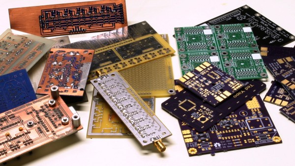
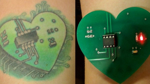
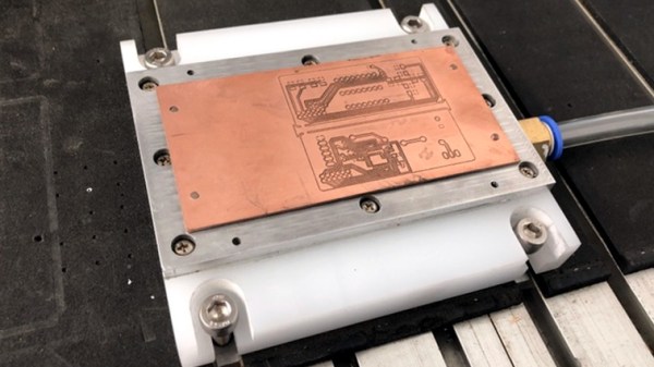
You’re only cool if you got chainz, so here’s some PCB chainz. This was done by [@jeffwurz] with OSHPark PCBs. The design, from as far as we can tell, is simple. It’s just a PCB without a soldermask, and a small cutout in one of the links. Assemble it into a chain, and if you’re clever, solder some resistor leads across the gap to make it a bit more solid.

ASMR, or officially, ‘autonomous sensory meridian response’, is the tingling sensation moving down your back induced by specific auditory (or visual) stimuli. That’s the scientific definition. On the Internet, it’s people breathing into microphones and smacking their lips. Yes, there are videos of this. Thousands of them. There are 11-year-old girls raking in the YouTube money posting ASMR videos. It’s weird and gross, and don’t get me started on slime videos. You’ve also got unboxing videos. The Raspberry Pi foundation found a way to combine ASMR with unboxing videos. I gotta respect the hustle here; ASMR and unboxing videos are some of the most popular content available, and the Pi foundation is not only combining the two, but doing so ironically. It’s exactly the content everyone wants to see, and it’ll bring in people who hate ASMR and unboxing videos. Someone over at the Pi foundation really knows what they’re doing here.

DIY Vacuum Table Enhances PCB Milling

CNC milling a copper-clad board is an effective way to create a PCB by cutting away copper to form traces instead of etching it away chemically, and [loska] has improved that process further with his DIY PCB vacuum table. The small unit will accommodate a 100 x 80 mm board size, which was not chosen by accident. That’s the maximum board size that the free version of Eagle CAD will process.

When it comes to milling PCBs, double-sided tape or toe clamps are easy solutions to holding down a board, but [loska]’s unit has purpose behind its added features. The rigid aluminum base and vacuum help ensure the board is pulled completely flat and held secure without any need for external fasteners or adhesives. It’s even liquid-proof, should cutting fluid be used during the process. Also, the four raised pegs provide a way to reliably make double-sided PCBs. By using a blank with holes to match the pegs, the board’s position can be precisely controlled, ensuring that the back side of the board is cut to match the front. Holes if required are drilled in a separate process by using a thin wasteboard.

Milling copper-clad boards is becoming more accessible every year; if you’re intrigued by the idea our own [Adil Malik] provided an excellent walkthrough of the workflow and requirements for milling instead of etching.