Creating A PCB In Everything: Upverter

For the last five months, I’ve been writing a series of posts describing how to build a PCB in every piece of software out there. Every post in this series takes a reference schematic and board, and recreates all the elements in a completely new PCB tool.

There are three reasons why this sort of review is valuable. First, each post in this series is effectively a review of a particular tool. Already we’ve done Fritzing (thumbs down), KiCad (thumbs up), Eagle (thumbs up), and Protel Autotrax (interesting from a historical perspective). Secondly, each post in this series is a quick getting started guide for each PCB tool. Since the reference schematic and board are sufficiently complex for 90% of common PCB design tasks, each of these posts is a quick how-to guide for a specific tool. Thirdly, this series of posts serves as a basis of comparison between different tools. For example, you can do anything you want in KiCad and most of what you want in Eagle. Fritzing is terrible, and Autotrax is the digital version of the rub-on traces you bought at Radio Shack in 1987.

With that introduction out of the way, let’s get cranking on Upverter.

A little bit about Upverter

Upverter was founded in 2010 as an entirely web-based EDA tool aimed at students, hobbyists, and Open Hardware circuit designers. This was one of the first completely web-based circuit design tools and Upverter’s relative success has been a bellwether for other completely web-based EDA tools such as circuits.io and EasyEDA.

I would like to take a second to mention Upverter is a Y Combinator company (W11), which virtually guarantees this post will make it to the top of Hacker News. Go fight for imaginary Internet points amongst yourselves.

Upverter is a business after all, so how are they making money? Most EDA suites offer a free, limited version for personal, hobbyist, and ‘maker’ projects, and Upverter is no exception. The professional tier offers a few more features including CAM export, 3D preview, an API, simulation (coming soon), BOM management, and unlimited private projects for $125 per seat per month, or $1200 per seat per year.

To give you a basis of comparison for that subscription fee, Eagle CAD’s new license scheme gives you everything – 999 schematic sheets, 16 layers, and unlimited board area – for $65 per month, or $500 per year. Altium’s CircuitStudio comes in at $1000 for a one-year license. There are more expensive EDA suites such as Altium Designer and OrCAD, but you have to call a sales guy just to get a price.

Upverter is positioning itself as a professional tool at a professional price. There are better tools out there, of course, but there are thousands of businesses out there designing products with tools that cost $500 to $1000 per seat per year. In any event, this is all academic; the Hackaday crowd gravitates towards the free end of the market, whether that means beer or speech.

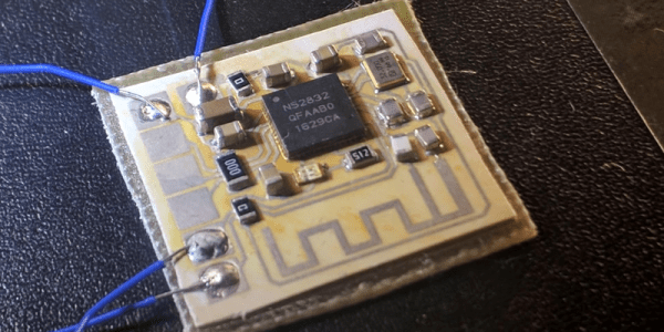
A big draw for Upverter is their Parts Concierge service. You’ll never have to create a part from scratch again, so the sales copy says. Apparently, Upverter is using a combination of very slick scripts to pull part layouts off a datasheet and human intervention / sanity check to create these parts. Does it work? We’re going to find out in the review below.

Continue reading “Creating A PCB In Everything: Upverter”

No-Etch: The Proof In The Bluetooth Pudding

In a previous episode of Hackaday, [Rich Olson] came up with a new no-etch circuit board fabrication method. And now, he’s put it to the test: building an nRF52 Bluetooth reference design, complete with video, embedded below.

The quick overview of [Rich]’s method: print out the circuit with a laser printer, bake a silver-containing glue onto the surface, repeat a few times to get thick traces, glue the paper to a substrate, and use low-temperature solder to put parts together. A potential drawback is the non-negligible resistance for the traces, but a lot of the time that doesn’t matter and the nRF52 reference design proves it.

The one problem here may be the trace antenna. [Rich] reports that it sends out a weaker-than-expected signal. Any RF design folks want to speculate wildly about the cause?

Continue reading “No-Etch: The Proof In The Bluetooth Pudding”

A Heart For His Girlfriend

[Decino] made a nice LED animated blinking heart box for his girlfriend. That’s a nice gesture, but more to the point here, it’s a nice entrée into the world of custom hardware. The project isn’t anything more than a home-etched PCB, a custom 3D-printed case, a mess of LEDs and current-limiting resistors, a shift register, and a microcontroller. (OK, we’re admittedly forgetting the Fifth Element.) The board is even single-sided with pretty wide traces. In short, it’s a great first project that ties together all of the basics without any parts left over. Oh, and did we mention Valentine’s day?

Once you’ve got these basics down, though, the world is your oyster. Building almost anything you need is just a matter of refining the process and practice. And if you’ve never played around with shift registers, a mega-blinker project like this is a great way to learn hands-on.

Not everything we write up on Hackaday has to be neural nets and JTAG ports. Sometimes a good beginner project that hits the fundamentals with no extra fat is just the ticket. What’s your favorite intro project?

PCB Design Guidelines To Minimize RF Transmissions

There are certain design guidelines for PCBs that don’t make a lot of sense, and practices that seem excessive and unnecessary. Often these are motivated by the black magic that is RF transmission. This is either an unfortunate and unintended consequence of electronic circuits, or a magical and useful feature of them, and a lot of design time goes into reducing or removing these effects or tuning them.

You’re wondering how important this is for your projects and whether you should worry about unintentional radiated emissions. On the Baddeley scale of importance:

  • Pffffft – You’re building a one-off project that uses battery power and a single microcontroller with a few GPIO. Basically all your Arduino projects and around-the-house fun.
  • Meh – You’re building a one-off that plugs into a wall or has an intentional radio on board — a run-of-the-mill IoT thingamajig. Or you’re selling a product that is battery powered but doesn’t intentionally transmit anything.
  • Yeeeaaaaahhhhhhh – You’re selling a product that is wall powered.
  • YES – You’re selling a product that is an intentional transmitter, or has a lot of fast signals, or is manufactured in large volumes.
  • SMH – You’re the manufacturer of a neon sign that is taking out all wireless signals within a few blocks.

Continue reading “PCB Design Guidelines To Minimize RF Transmissions”

Print Flexible PCBs With A 3D Printer

Let’s get it out of the way right up front: you still need to etch the boards. However, [Mikey77] found that flexible plastic (Ninjaflex) will adhere to a bare copper board if the initial layer height is set just right. By printing on a thin piece of copper or conductive fabric, a resist layer forms. After that, it is just simple etching to create a PCB. [Mikey77] used ferric chloride, but other etchants ought to work, as well.

Sound simple, but as usual, the devil is in the details. [Mikey77] found that for some reason white Ninjaflex stuck best. The PCB has to be stuck totally flat to the bed, and he uses spray adhesive to do that. Just printing with flexible filament can be a challenge. You need a totally constrained filament path, for one thing.

Continue reading “Print Flexible PCBs With A 3D Printer”

Hackaday Links: January 8, 2017

What do you get when mindless automatons with no capacity for reason or logic converse? While you discuss that in the comments, here are two chatbots on Twitch. The highlights? A few hours ago they were doing the cutesy couple, “‘I love you more!’, ‘No, I love you more!'” thing. This was ended by, “Error, cannot connect to server.” Even robot love is not eternal.

3D printer nozzles wear out. Put a few hundred hours on a brass nozzle, and you’re not going to get the same print quality as when you started. This has led to stainless and silly-con carbide nozzles. Now there’s a ruby nozzle. It’s designed by [Anders Olsson], the same guy who’s using an Ultimaker to print neutron shielding. This guy is a nuclear engineer, and he knows his stuff. This is a nozzle designed to not grind contaminants into extruded plastic, and it looks cool, too.

This is the eighth day of the year, but the guild of independent badge makers of DEF CON are already hard at work. AND!XOR is working on the DC25 badge, that promises to be bigger, badder, and more Bender. I’m loving the Hunter S. Bender theme.

Anyone can design a PCB, but how do you panelize multiple PCBs? There’s a lot to consider – routing, mouse bites, and traces for programming the board while still panelized. This is the best solution we’ve seen. It’s a GUI that allows you to organize Gerbers on a panel, rotate them, add routes and cutouts, and generally do everything a board house does. It’s all Open Source and everything is available on GitHub.

[ducksauz] found a very old ‘computer trainer’ on eBay. It’s a DEC H-500, built to explain the basics of digital electronics and semiconductors to a room full of engineering students. It is an exceptionally beautiful piece of equipment with lovely hand-drawn traces and ‘surface mounted’ 7400 chips mounted on the back side.

Building Beautiful Boards With Star Simpson

Over the last decade or so, the cost to produce a handful of custom PCBs has dropped through the floor. Now, you don’t have to use software tied to one fab house – all you have to do is drop an Eagle or KiCad file onto an order form and hit ‘submit’.

With this new found ability, hackers and PCB designers have started to build beautiful boards. A sheet of FR4 is no longer just a medium to populate parts, it’s a canvas to cover in soldermask and silkscreen.

Over the last year, Star Simpson has been working on a project to make electronic art a reality. Her Circuit Classics take the original art from Forrest Mims’ Getting Started In Electronics notebooks and turn them into functional PCBs. It’s a kit, an educational toy, and a work of art on fiberglass, all in one.

At the 2016 Hackaday Superconference, Star gave her tips and tricks for producing beautiful PCBs. There’s a lot going on here, from variable thickness soldermasks, vector art on a silkscreen, and even multicolored boards that look more at home in an art gallery than an electronics workbench.

Continue reading “Building Beautiful Boards With Star Simpson”