Clock Of Clocks Expands, Goes Digital

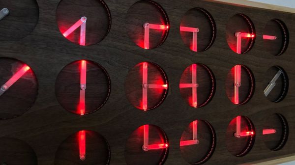
Some people just want to have their cake and eat it too, but very few of us ever get to pull it off. [Erich Styger] has, though with V5 of his “MetaMetaClock”— a clock made of clocks, that uses the orientation of the hands to create digits.

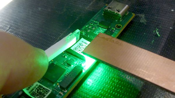
We’ve seen previous versions of this clock. As before, the build is exquisitely detailed and all relevant files are on GitHub. This version keeps the acrylic light-pipe hands of version 4, but adds more of them: 60 clocks vs 24. Larger PCBs are used, grouping the dual-shaft steppers into groups of four, instead of the individual PCBs used before. Each PCB has an NXP LPC845 (a Cortex M0 microcontroller) that communicates on an RS-485 bus. Placing four steppers per microcontroller reduces parts count somewhat compared to previous versions (which had each ‘clock’ on its own modular PCB) albeit at the cost of some flexibility.

While the last version used veneers on its face, this version is cut by CNC by from a large slab of oak. It’s certainly the most attractive version yet, and while bigger isn’t always better, more clock faces means more potential effects. Date? Time? Block letters? Arbitrary text? Kaleidoscopic colours from the RGB LEDs? It’s all there, and since it’s open source, anyone who builds one can add more options. A BLE interface makes it quick and easy to wirelessly switch between them or set the time.

It’s nice sometimes to watch projects like this improve incrementally over time. [Erich] mentions that he plans to add Wifi and a web-based user interface for the next version. We look forward to it, and are grateful to  [jicasi] for the tip. Just as it is always clock time at Hackaday, so you can always toss a tip of your own into the box.

Continue reading “Clock Of Clocks Expands, Goes Digital”

Homebrew Electron Beam Lithography With A Scanning Electron Microscope

If you want to build semiconductors at home, it seems like the best place to start might be to find a used scanning electron microscope on eBay. At least that’s how [Peter Bosch] kicked off his electron beam lithography project, and we have to say the results are pretty impressive.

Now, most of the DIY semiconductor efforts we’ve seen start with photolithography, where a pattern is optically projected onto a substrate coated with a photopolymer resist layer so that features can be etched into the surface using various chemical treatments. [Peter]’s method is similar, but with important differences. First, for a resist he chose poly-methyl methacrylate (PMMA), also known as acrylic, dissolved in anisole, an organic substance commonly used in the fragrance industry. The resist solution was spin-coated into a test substrate of aluminized Mylar before going into the chamber of the SEM.

As for the microscope itself, that required a few special modifications of its own. Rather than rastering the beam across his sample and using a pattern mask, [Peter] wanted to draw the pattern onto the resist-covered substrate directly. This required an external deflection modification to the SEM, which we’d love to hear more about. Also, the SEM didn’t support beam blanking, meaning the electron beam would be turned on even while moving across areas that weren’t to be exposed. To get around this, [Peter] slowed down the beam’s movements while exposing areas in the pattern, and sped it up while transitioning to the next feature. It’s a pretty clever hack, and after development and etching with a cocktail of acids, the results were pretty spectacular. Check it out in the video below.

It’s pretty clear that this is all preliminary work, and that there’s much more to come before [Peter] starts etching silicon. He says he’s currently working on a thermal evaporator to deposit thin films, which we’re keen to see. We’ve seen a few sputtering rigs for thin film deposition before, but there are chemical ways to do it, too.

Continue reading “Homebrew Electron Beam Lithography With A Scanning Electron Microscope”

Tiny Prisms Let You See What Lies Beneath A BGA Chip

Compared to through-hole construction, inspecting SMD construction is a whole other game. Things you thought were small before are almost invisible now, and making sure solder got where it’s supposed to go can be a real chore. Add some ball grid array (BGA) chips into the mix, where the solder joints are not visible by design, and inspection is more a leap of faith than objective proof of results.

How it works.

Unless, of course, you put the power of optics to work, as [Petteri Aimonen] does with this clever BGA inspection tool. It relies on a pair of tiny prisms to bounce light under one side of a BGA chip and back up the other. The prisms are made from thin sheets of acrylic; [Petteri] didn’t have any 1-mm acrylic sheet on hand, so he harvested material from a razor blade package. The edge of each piece was ground to a 45-degree angle and polished with successively finer grits until the surfaces were highly reflective. One prism was affixed to a small scrap of PCB with eleven SMD LEDs in a row, forming a light pipe that turns the light through 90 degrees. The light source is held along one edge of a BGA, shining light underneath to the other prism, bouncing light through the forest of solder balls and back toward the observer.

The results aren’t exactly crystal clear, which is understandable given the expedient nature of the materials and construction employed. But it’s certainly more than enough to see any gross problems lying below a BGA, like shorts or insufficiently melted solder. [Petteri] reports that flux can be a problem, too, as excess of the stuff can crystalize between pads under the BGA and obstruct the light. A little extra cleaning should help in such cases.

Haven’t tackled a BGA job yet? You might want to get up to speed on that.

RCA’s Clear Plastic TV Wowed Crowds In 1939

In the United States in 1939, television sets still had a long way to go before they pretty much sold themselves. Efforts to do just that are what led to RCA’s Lucite Phantom Telereceiver, which aimed to show people a new way to receive broadcast media.

Created for the 1939 World’s Fair, the TRK-12 Lucite Phantom Telereceiver introduced people to the concept of television. Production models were housed in contemporary wood cabinets, but the clear acrylic (itself also a relatively new thing) units allowed curious potential customers to gaze within, and see what was inside these devices.

One interesting feature is the vertically-mounted cathode ray tube, which reflects off a mirror in the top cover of the cabinet for viewing. This meant that much of the bulk of the TRK-12 could be vertical instead of horizontal. Important, because the TRK-12 was just over a meter tall and weighed 91 kilograms (or just over 200 lbs.)

Clearly a luxury item, the TRK-12 sold for $600 which was an eye-watering sum for the time. But it was a glimpse of the future, and as usual, the future is made available a few ticks early to those who can afford the cost.

Want to see one in person? You might be in luck, because an original resides at the MZTV Museum of Television in Toronto, Canada.

Stop Silicone Cure Inhibition, No Fancy Or Expensive Products Required

Casting parts in silicone is great, and 3D printing in resin is fantastic for making clean shapes, so it’s natural for an enterprising hacker to want to put the two together: 3D print the mold, pour in the silicone, receive parts! But silicone’s curing process can be inhibited by impurities. What’s cure inhibition? It’s a gross mess as shown in the image above, that’s what it is. Sadly, SLA-printed resin molds are notorious for causing exactly that. What’s a hacker to do?

Firstly: there are tin-cure and platinum-cure silicones, and for the most part tin-cure silicone works just fine in resin-printed molds. Platinum-cure silicones have better properties, but are much more susceptible to cure inhibition. Most workarounds rely on adding some kind of barrier coating to molds, but [Jan Mrázek] has a cheap and scalable method of avoiding this issue that we haven’t seen before. Continue reading “Stop Silicone Cure Inhibition, No Fancy Or Expensive Products Required”

fiber matrix

Big LED Matrix Becomes Tiny LED Matrix Thanks To Fiber Optics

Everyone loves LED matrices, and even if you can’t find what you like commercially, it’s pretty easy to make just what you want. Need it big? No problem; just order a big PCB and some WS2812s. Need something tiny? There are ridiculously small LEDs that will test your SMD skills, as well as your vision.

But what if you want a small matrix that’s actually a big matrix in disguise? For that, you’ll want to follow [elliotmade]’s lead and incorporate fiber optics into your LED matrix. The build starts with a 16×16 matrix of WS2812B addressable LEDs, with fairly tight spacing but still 160 mm on a side. The flexible matrix was sandwiched between a metal backing plate and a plastic bezel with holes directly over each LED. Each hole accepts one end of a generous length of flexible 1.5-mm acrylic light pipe material; the other end plugs into a block of aluminum with a 35 by 7 matrix of similar holes. The small block is supported above the baseplate by standoffs, but it looks like the graceful bundle of fibers is holding up the smaller display.

A Raspberry Pi Pico running a CircutPython program does the job of controlling the LEDs, and as you can see in the video below, the effect is quite lovely. Just enough light leaks out from the fibers to make a fascinating show in the background while the small display does its thing. We’ve seen a few practical uses for such a thing, but we’re OK with this just being pretty. It does give one ideas about adding fiber optics to circuit sculptures, though.

Continue reading “Big LED Matrix Becomes Tiny LED Matrix Thanks To Fiber Optics”

Clock-of-Clocks Adds Light-Pipe Hands For Beauty And Function

We’ve gotten used to seeing “meta clocks,” clocks that use an array of analog clock faces and piece together characters using the hands of the clocks. They’re very clever, and we always like to see them, especially when they come with detailed build instructions like this one does.

What’s also nice about [Erich Styger]’s “MetaClockClock” display is the twist on the original concept. Where most clock-of-clocks depend on the contrast between the hands and the faces of the analog movements, [Erich] added light to the mix. Hidden inside the bezel of each clock is a strip of RGB LEDs; coupled with the clear acrylic hands of the clock, which act as light pipes, each clock can contribute different shapes of different colors to the display. Each clock is built around a dual-shaft stepper motor of the kind used in car dashboard gauges; the motors each live on a custom PCB, while the LEDs are mounted on a ring-shaped PCB of their own. Twenty-four of the clocks are mounted in a very nice walnut panel, which works really well with the light-pipe hands. The video below shows just some of the display possibilities.

[Erich] has documented his build process in extreme detail, and has all the design files up on GitHub. We won’t say that recreating his build will be easy — there are a lot of skills needed here, from electronics to woodworking — but at least all the information is there. We think this is a beautiful upgrade to [Erich]’s earlier version, and we’d love to see more of these built.

Continue reading “Clock-of-Clocks Adds Light-Pipe Hands For Beauty And Function”