Just How Dodgy Are Cheap USB Chargers Anyway?

Aside from apparently having both the ability to reproduce on their own and simultaneously never being around when you need one, USB chargers seem innocuous enough. The specs are simple: convert mains voltage to 5 volts, and don’t kill anyone while doing it. Both specs are typically met by most designs, but judging by [DiodeGoneWild]’s latest USB charger teardown, the latter only just barely, and with a whole lot of luck.

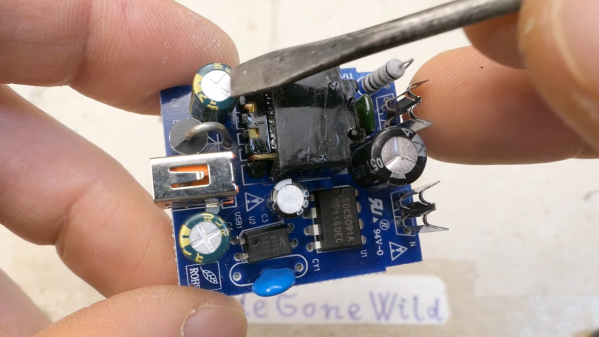
The sad state of plug-in USB power supplies is one of [DiodeGoneWild]’s pet gripes, and deservedly so. Most USB chargers cram a lot of electronics into a mighty small volume, and are built to a price point, meaning that something has to give in the design. In the case of the two units he tears apart in the video below, it’s pretty clear where the compromises are. Neither unit met the specs on the label in terms of current supplied and voltage regulation, even the apparently more capable quick charger, which is the first to go under the knife. The PCB within holds some alarming surprises, like the minimal physical isolation between the mains part of the circuit and the low-voltage section, but the real treat is the Schottky diode that gets up to 170°C under full load. Safety tip: when you smell plastic burning, throw the thing out.

The second charger didn’t fare any better; although it didn’t overheat, that’s mainly because it shut itself off before it could deliver a fraction of its rated 1 amp output. The PCB construction was shoddy in the extreme, with a squiggly trace standing in for a proper fuse and a fraction of a millimeter separation between primary and secondary traces. The flyback transformer was a treat, too; who doesn’t want to rely on a whisper-thin layer of cheap lacquer to keep mains voltage out of your phone?

All in all, these designs are horrible, and we have to thank [DiodeGoneWild] for the nightmares we’ll have whenever we plug into one of these things from now on. On the other hand, this was a great introduction to switch-mode power supply designs, and what not to do with our own builds. Continue reading “Just How Dodgy Are Cheap USB Chargers Anyway?” →
Vector Network Analyzer Demo And Teardown

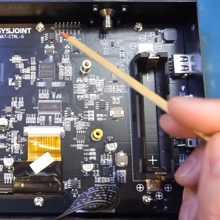
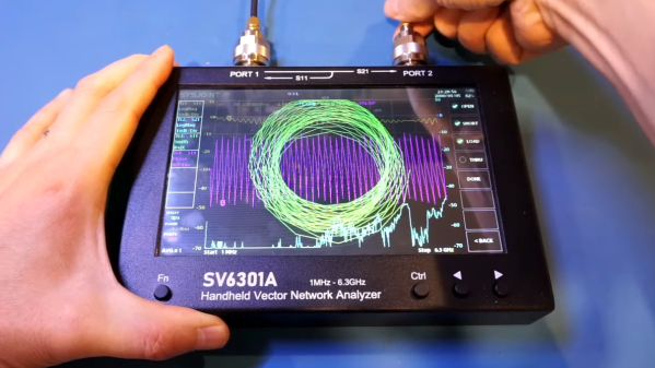
[Kerry Wong], ever interested in trying out and tearing down electrical devices, demonstrates and examines the SV 6301a Handheld Vector Network Analyzer. He puts the machine through its paces, noting that the 7 inch touchscreen is a pretty nice feature for those whose eyesight isn’t quite what it used to be.

The internals are similar to the nanoVNA-F V3, but not identical.

What’s a Vector Network Analyzer (VNA)? It’s not for testing Ethernet or WiFi. It’s aimed at a more classical type of “network”. The VNA tests and evaluates characteristics of electrical networks, especially as related to RF and microwave.

It provides detailed information about properties across a specified frequency range, making it an indispensable tool for advanced work. Tektronix has a resource page that goes into detail about exactly what kinds of things a VNA is good for.

[Kerry] shows off a few different features and sample tests before pulling the unit apart. In the end, he’s satisfied with the features and performance of the device, especially the large screen and sensible user interface.

After all, not every piece of test equipment does a great job at fulfilling its primary function, like the cheap oscilloscope that was a perhaps a little too cheap.

Continue reading “Vector Network Analyzer Demo And Teardown” →

Turning Soviet Electronics Into A Nixie Tube Clock

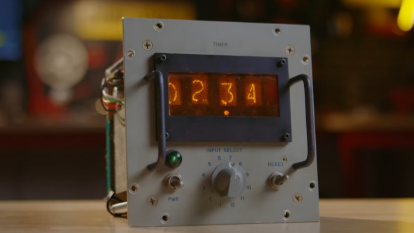
Sometimes you find something that looks really cool but doesn’t work, but that’s an opportunity to give it a new life. That was the case when [Davis DeWitt] got his hands on a weird Soviet-era box with four original Nixie tubes inside. He tears the unit down, shows off the engineering that went into it and explains what it took to give the unit a new life as a clock.

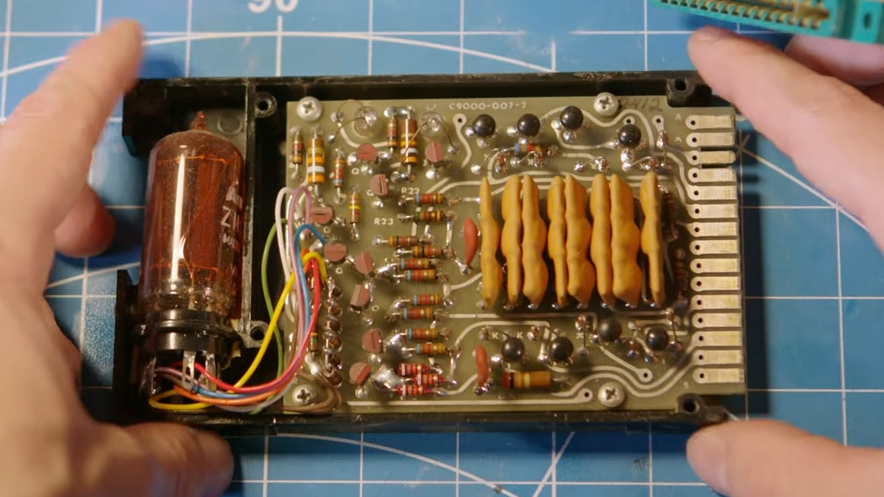
Each digit is housed inside a pluggable unit. If a digit failed, a technician could simply swap it out.

A lot can happen over decades of neglect. That was clear when [Davis] discovered every single bolt had seized in place and had to be carefully drilled out. But Nixie tubes don’t really go bad, so he was hopeful that the process would pay off.

The unit is a modular display of some kind, clearly meant to plug into a larger assembly. Inside the unit, each digit is housed in its own modular plug with a single Nixie tube at the front, a small neon bulb for a decimal point, and a bunch of internal electronics. Bringing up the rear is a card edge connector.

Continues after the break…

Continue reading “Turning Soviet Electronics Into A Nixie Tube Clock” →

Tivoli Teardown Disappoints

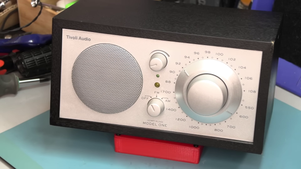
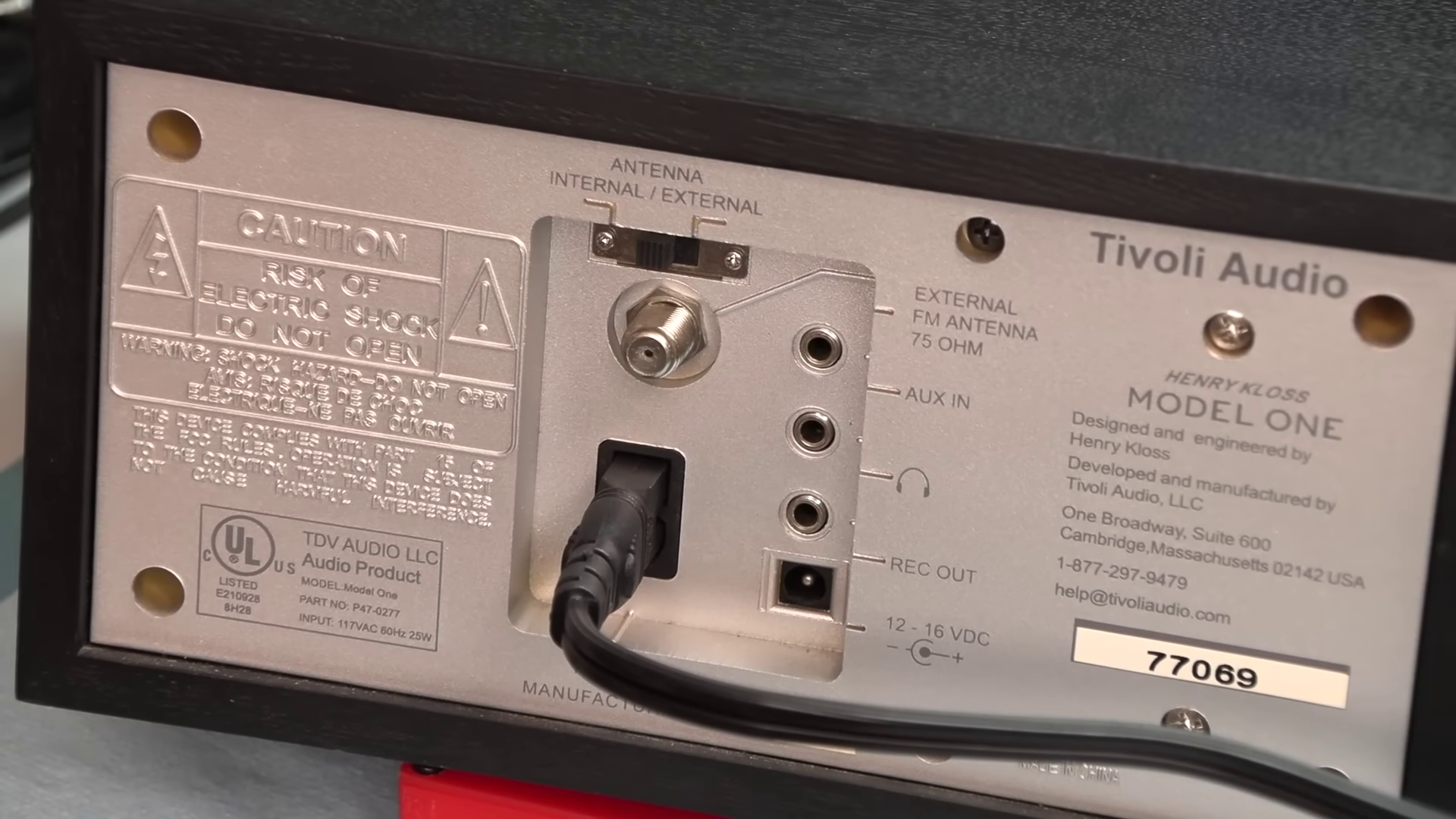
[Fran] has been curious about the innards of Tivoli Audio’s Model One radio, but was reluctant to shell out $200 just to tear it apart. But she found one recently on eBay, won the auction, and proceeded to do a review and teardown. Spoiler alert, she was disappointed.

Physically speaking, the radio looks great and has quite an array of I/O connections. The geared tuning knob looks cool, but is heavily damped which [Fran] isn’t keen about. Turning it on, a few more quirks are discovered. The volume control is out-of-whack — it appears they substituted a linear taper potentiometer where a logarithmic taper was called for.

Another problem, at least in the RF-dense metropolitan areas like Philadelphia, is the FM tuner’s station-lock feature. It is so strong that it can be impossible to tune in weak stations. This is especially ironic since, according to Wikipedia, that was one of audio engineer Henry Kloss’s main goals when founding Tivoli Audio back in 2000:

Their first product was the Model One, a simple to use mid-century modern designed table top radio with a high-performance tuner, receiving FM radio in congested urban locations, while maintaining the ability to pick out distant or low power stations. Kloss had noted that the mid 60’s wave of Japanese radios lacked the ability to receive FM stations in congested locations, and this became a defining goal of his radio designs throughout his career.

Interestingly, many folks in the YouTube comments say their Model One radios have none of these issues. We wonder if [Fran] has obtained a damaged radio, or maybe a newer version produced with less attention to detail. If you have a broken Model One radio, before tossing it, consider the hack we wrote about last year, turning it into an internet radio.

Continue reading “Tivoli Teardown Disappoints” →

Tearing Down And Improving A Professional Power Supply

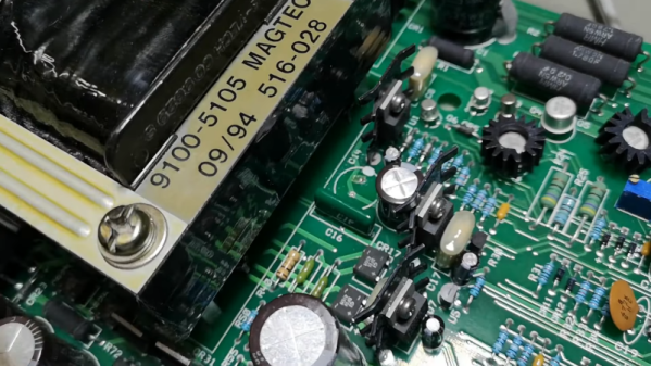
[OZ2CPU] has an HP power supply that is about 30 years old. It looks brand new, though, and has three outputs and includes tracking for the adjustable positive and negative supply. After a quick demo of the unit’s features, he tears it all down so we can see inside. You can catch the video below.

Some similar supplies offer a 10-turn adjustment knob, but this one doesn’t. Inside is a beefy transformer and quite a few through-hole components. There was room to change the main adjusted pot to a 10-turn unit, so he made the mod.

Continue reading “Tearing Down And Improving A Professional Power Supply” →

Teardown Of An Aircraft Video Symbol Generator

[Adrian Smith] recently scored an avionics module taken from a British Aerospace 146 airliner and ripped it open for our viewing pleasure. This particular aircraft was designed in the early 1980s when the electronics used to feed the various displays in the cockpit were very different from modern designs. This particular box is called a ‘symbol generator’ and is used to generate the various real-time video feeds that are sent to the cockpit display units. Various instruments, for example, the weather radar, feed into it, and it then reformats the video if needed, mixing in any required additional display.

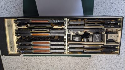
Top view of the symbol generator instrument rack

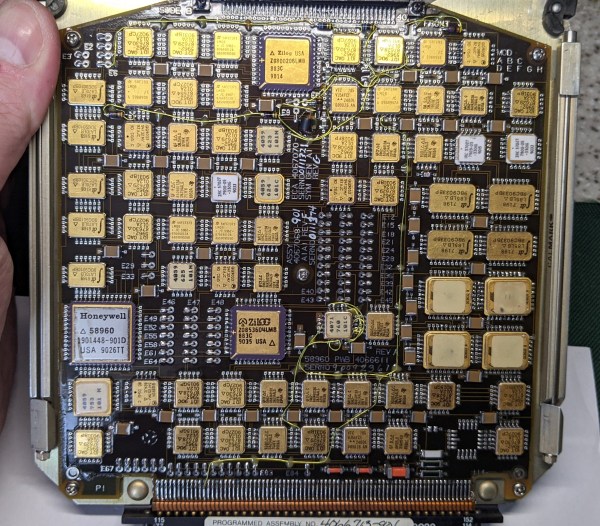
There are many gold-plated chips on these boards, which indicates these may be radiation-hardened versions of familiar devices, most of which are 54xx series logic. 54xx series logic is essentially the same functionally as the corresponding 74xx series, except for the much wider operating temperature range mandated by military and, by extension, commercial aviation needs. The main CPU board appears to be based around the Intel 8086, with some Zilog Z180 compatible processors used on the two video display controller boards. We noted the Zilog Z0853604, which is their counter/timer/GPIO chip. Obviously, there are many custom ASICs produced by Honeywell as well as other special order items that you’ll never find the datasheet for. Now there’s a challenge!

Finally, we note the standard 400 Hz avionics-standard power supply, which, as some may know, is the standard operating frequency for the AC power system used within modern aircraft systems. The higher frequency (compared to 50 or 60 Hz) means the magnetic components can be physically smaller and, therefore, lighter for a given power handling capability.

We see a lot of avionics teardowns, likely because they’re fascinating. Here’s some more British military gear, an interesting RF distance measuring box from the 1970s, and finally, some brave soul building their own avionics gear. What could possibly go wrong?

Continue reading “Teardown Of An Aircraft Video Symbol Generator” →

Google Nest Hub Teardown

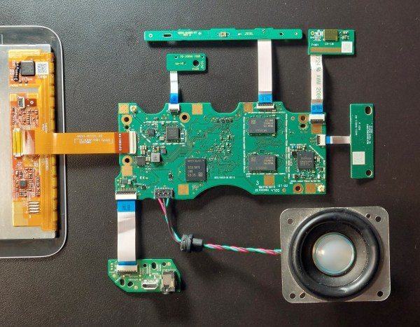
Seeing the guts of devices is a fascination that many hackers share. [Txyz] tore down a 2nd gen Google Nest Hub for all of us to enjoy. The video after the break is well produced and relaxing to watch as various heat shields are removed and debug cables are soldered on.

The main SOC is an Amlogic S905D3G, a 4-core A55-based SoC. The important chips are meticulously documented, and it’s a fascinating look inside a device common in many people’s homes. One chip that’s of note is the BGT60TR13C, otherwise known as Project Soli. It is an 8x10mm chip that uses radar to detect movement with sub-millimeter accuracy. This allows the device to measure your sleep quality or recognize gestures. Luckily for us, [Txyz] has included a datasheet and a block diagram. First, the chip fills a FIFO with data samples. Once full, it will issue an interrupt to the main SoC, which empties the buffer via SPI.

The debug cables allowed him to capture traces of the SPI commands to the BGT60TR13C. [Txyz] focused on decoding the various data blocks and the configuration registers. Unfortunately, only a few registers are documented in the datasheet, and it isn’t apparent what they do.

If a hardware teardown isn’t enough for you, perhaps a software teardown to bypass Secure Boot might sate your interest.

Continue reading “Google Nest Hub Teardown” →