Come For The PCB Holder, Stay For The Tour Of FreeCAD

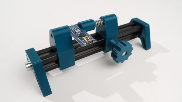
PCB holders are great tools. Not only is the PCB Solder Fren from [PistonPin] a nice DIY design, it offers some insight into the parts design process with FreeCAD.

This design nicely demonstrates FreeCAD’s workflow for designing parts.

The PCB holder uses 3D-printed parts, M5 hardware, a length of 2020 aluminum extrusion, and one spring to create a handy and adjustable design that accommodates a variety of PCB sizes and shapes. If the ends of the extrusion are threaded, the end caps can be screwed in. Otherwise, a little glue ought to do the trick.

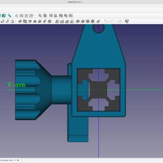
Want a little more insight into what making a part like this involves? [Jo Hinchliffe] at FreeCAD reached out to [PistonPin] for more detail and has a blog post explaining the workflow and steps involved in this part. As a bonus, STEP files and the FreeCAD project file are all included!

Not only is FreeCAD simple to use, but it’s also flexible enough to accommodate custom, niche extensions like a Rocketry workbench, so be sure to give it a look for your open-source CAD needs.

You Can Now Order A Brand-New Amiga PCB

The Commodore 64 has been pulled apart, reverse engineered, replicated, and improved upon to no end over the last four decades or so. The Amiga 500 has had less attention, in part due to its greater level of sophistication. However, you can now order a brand-new Amiga-compatible PCB if you’re looking to put together a machine from surplus parts.

The design is known as Denise, and is apparently the work of an anonymous Swedish designer according to the Tindie listing. It’s not a direct replica of any one Amiga machine. Instead, it’s best described as “a compact A500+ compatible motherboard with two Zorro2 slots and a few additional features.”

Denise is just a PCB, though. No emulated chips or other components are included. To use the PCB, you’ll need a full set of Amiga custom chips and a suitable Motorola 68000-series CPU to suit. It can be used with either OCS or ECS chipsets. At this stage, it’s only verified to work with the 2MB version of the Agnus chip, though the creators believe it should work with a 1MB “Diet Agnus.”  Some modern conveniences are on hand, too. A pair of microcontrollers will allow the use of Amiga or PC keyboards, along with Amiga or PS/2 style mice, including support for scroll wheels.

Given the number of damaged, battered, and corroded Amiga PCBs out there, it’s great that there is a source of fresh, new PCBs for restoration purposes. Video after the break.

Continue reading “You Can Now Order A Brand-New Amiga PCB”

Designing A PCB GPS Antenna From Scratch

These days, when it comes to GPS devices the antenna is typically part of the package. But what better opportunity for [Pepijn] to learn how to make a GPS antenna from scratch for a badge add-on?

A patch antenna is an antenna of a flat design, which [Pepijn] was going to put directly on a PCB. However, there was added complexity due to GPS being a circularly polarized signal, and that meant doing some research.

Sadly, nowhere did [Pepijn] encounter a straightforward reference design or examples, but in the end success came from going with a truncated corner patch antenna design and using simulation software to figure out exactly what dimensions were needed. (The openEMS free simulation software didn’t bring success, but the non-free Sonnet with a trial license did the trick.) The resulting PCB may not look particularly complex, but every detail matters in such designs.

KiCad handled the PCB CAD design but the prototype came from cutting the PCB on a CNC machine instead of having it fabricated and shipped; a much cheaper and faster option for those with access to the right tools. A bit more testing had the prototype looking good, but the real proof came when it successfully received GPS signals and spewed valid NMEA messages. The design files are on GitHub but as [Pepijn] says, the project was about the journey more than anything else.

Silicon Photolithography The PCB Way

[ProjectsInFlight] has been doing some fantastic work documenting his DIY semiconductor fab lately. Next up: exploring down-and-dirty photolithography methods.

If you’ve been following along with this series — and why wouldn’t you? — you’ll recall [ProjectsInFlight]’s earlier experiments, like creating oxide layers on silicon chips with a homebrew tube furnace and exploring etchants that can selectively remove them. But just blasting away the oxide layer indiscriminately isn’t really something you need to do when etching the fine features needed to fabricate a working circuit. The trouble is, most of the common photoresist solutions used by commercial fabs are unobtainium for hobbyists, leading to a search for a suitable substitute.

Surprisingly, PCB photoresist film seemed to work quite well, but not without a lot of optimization by [ProjectsInFlight] to stick it to the silicon using a regular laminator. Also in need of a lot of tweaking was the use of a laser printer to create masks for the photolithography process on ordinary transparency film, including the surprisingly effective method of improving the opacity of prints with acetone vapor. There were also extensive experiments to determine the best exposure conditions, a workable development process, and the right etchants to use. Watch the video below for a deep dive into all those topics as well as the results, which are pretty good.

There’s a lot to be said for the methodical approach that [ProjectsInFlight] is taking here. Every process is explored exhaustively, with a variety of conditions tested before settling on what works best. It’s also nice to see that pretty much all of this has been accomplished with the most basic of materials, all of which are easily sourced and pretty cheap to boot. We’re looking forward to more of the same here, as well as to see what others do with this valuable groundwork.

Continue reading “Silicon Photolithography The PCB Way”

PCB Repair Is A Sticky Proposition

What do you do when a PCB is cracked or even broken in two? [MH987] has a plan: superglue the board back and then bridge the traces with solder, solder paste, or wire. The exact method, of course, depends on the extent of the damage.

We’ve had some success with similar techniques, and, honestly, for single-sided boards, we would be tempted to add a thin backer behind the crack. We’ve also used conductive paint to repair traces, but it’s good to have having as many tricks as possible because you never know what will work best for a particular repair. The post mentions that this is easier to do on a single-sided board, but it is certainly possible to do on a two-layer board.

The example repair is a Walkman which — if you are a youngster — was a portable music player that takes cassette tapes. These haven’t been made since 2010, so it is important to repair what you have.

If you can’t repair your Walkman, you could build an updated version. If your board is seriously damaged, you might get hope from this more extreme repair.

An In-Depth Comparison Of Hobby PCB Manufacturers

[Icamtuf] has been working on a prototyping run of a project, which involves getting PCBs made by several low volume PCB manufacturing companies. After receiving the boards, he analyzed the results and produced an interesting analysis.

The project he is working on is Sir-Box-A-Lot, a Sokoban gaming console clone that we’ve covered before. It uses an AVR128DA28 microcontroller to emulate the original box-pushing game and drive the OLED display. He ordered PCBs from OSHPark, DigiKey Red, JLCPCB, PCBWay and Aisler.

OSHPark boards are gorgeous, but you pay for it.

There were pros and cons for each of the services: OSHPark produced the nicest-looking boards, but at the highest cost. DigiKey Red had a flawless solder mask, but a rather sloppy-looking silkscreen and shipped the boards covered in adhesive gunk. JLCPCB was fast, shipping the boards in less than 7 days, but the smaller details of the silkscreen were blurry and the solder mask was thinner than the others. The solder mask from PCBWay was very slightly misaligned but was thicker than most, and they were the only ones who queried a badly shaped hole to see what [Icamtuf] wanted to do: the others just made assumptions and made the boards without checking.

To be fair, this analysis is based on a single PCB design ordered once and it is possible that some companies were having a bad day. These were also delivered to the US, so your delivery times may vary. So, there are no clear winners and I wouldn’t make a choice based on this alone. But the analysis is well worth a read if you want to know what to look out for on your own PCBs.

Review: LibrePCB Hits Version 1.0

Nearly three years ago at the start of 2020 and before the pandemic hit, we took a look at an up-and-coming player in the world of PCB design. LibrePCB is by no means as old as the more established players, but at the time it was joining the ranks of open-source EDA packages with its first early stable releases. It showed a lot of promise but was still a little rough around the edges back then, but in the years since it’s advanced to the extent that in September they released version 1.0. That’s a significant moment for any open source package, so it’s time to return and take another look. It’s a cross-platform package with builds available for Linux, Windows, MacOS and FreeBSD, of which I needed the Linux version. There are one or two options to choose from, I went for the appImage as probably the least trouble. Very quickly I was in a new EDA package, and I set out to make a simple Schmitt trigger oscillator as a test project. Continue reading “Review: LibrePCB Hits Version 1.0”