Around 2010 or so, Samsung cameras came with an online service: Social Network Services. It enabled pictures to be unloaded wirelessly to social media with minimum hassle, which back then wasn’t quite as easily accomplished as it is today. Sadly they shuttered the service in 2021, leaving that generation of cameras, like so many connected devices, orphaned. Now along comes [Ge0rG] with a replacement, replicating the API on a $20 LTE dongle.
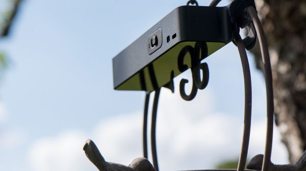
The dongle in question is one we featured a couple of years ago, packing a Linux-capable computer of similar power to a Raspberry Pi Zero alongside its cell modem. The camera can connect to the device, and a photo can be sent in a Mastodon post. It’s something of a modern version of the original, but for owners of the affected cameras it’s a useful recovery of a lost service.
It’s surprising in a way that we’ve not heard of more hacks using these dongles, as they do represent a useful opportunity. That we haven’t should be seen as a measure of the success of the Raspberry Pi and other boards like it, just as it’s no longer worth hacking old routers for Linux hardware projects, so there’s less of a need to do the same here.


