Secret Ingredient For 3D-Printed Circuit Traces: Electroplating

Conductive filament exists, but it takes more than that to 3D print something like a circuit board. The main issue is that traces made from conductive filament are basically resistors; they don’t act like wires. [hobochild]’s interesting way around this problem is to use electroplating to coat 3D-printed traces with metal, therefore creating a kind of 3D-printed circuit board. [hobochild] doesn’t yet have a lot of nitty-gritty detail to share, but his process seems fairly clear. (Update: good news! here’s the project page and GitHub repository with more detail.)

The usual problem with electroplating is that the object to be coated needs to be conductive. [hobochild] addresses this by using two different materials to create his test board. The base layer is printed in regular (non-conductive) plastic, and the board’s extra-thick traces are printed in conductive filament. Electroplating takes care of coating the conductive traces, resulting in a pretty good-looking 3D-printed circuit board whose conductors feature actual metal. [hobochild] used conductive filament from Proto-pasta and the board is a proof-of-concept flashing LED circuit. Soldering might be a challenge given the fact that the underlying material is still plastic, but the dual-material print is an interesting angle that even allows for plated vias and through-holes.

We have seen conductive filament used to successfully print workable electrical connections, but applications are limited due to the nature of the filament. Electroplating, a technology accessible to virtually every hacker’s workbench, continues to be applied to 3D printing in interesting ways and might be a way around these limitations.

Slick Keyboard Built With PCB Magic

Sometimes a chance conversation leads you to discover something cool you’ve not seen before, and before you know it, you’re ordering parts for yet another hardware build. That’s what happened to this scribe the other day when chatting on some random discord, to QMK maintainer [Nick Brassel aka tzarc] about Djinn, a gorgeous 64-key split mechanical keyboard testbed. It’s a testbed because it uses the newest STM32G4x microcontroller family, and QMK currently does not have support for this in the mainline release. For the time being, [Nick] maintains a custom release, until it gets merged.

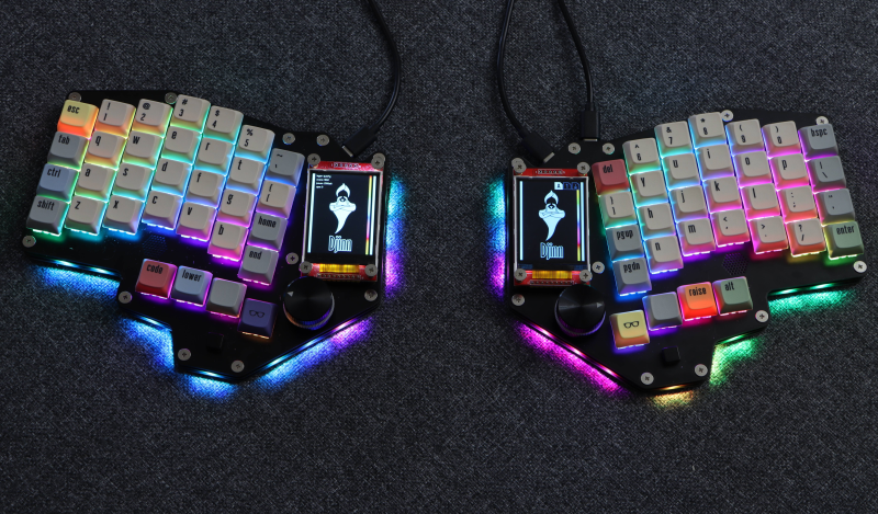
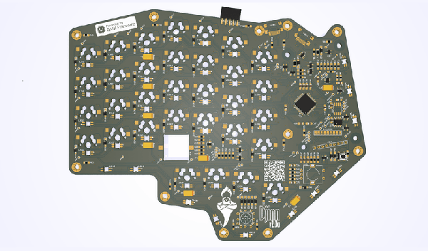
Hardware-wise, the design is fabulous, with a lot of attention to detail. We have individual per-key RGB LEDs, RGB underglow, a rotary encoder, a five-way tactile thumb switch, and a 240×320 LCD per half. The keyboard is based on a three PCB stack, two of which are there purely for structure. This slick design has enough features to keep a fair few of us happy.

Interestingly, when you look at the design files (KiCAD, naturally) [Nick] has chosen to take a mirrored approach to the PCB. That means the left and right sides are actually the same PCB layout. The components are populated on different sides of the PCB depending on which half you’re looking at! By mirroring footprints on both PCB sides, and hooking everything up in parallel, it’s possible to do it all with a single master layout.

This is a simple but genius idea that this scribe hadn’t come across before (the shame!) Secondarily it keeps costs down, as your typical Chinese prototyping house will not deal in PCB quantities below five, so you can make two complete keyboards on one order, rather than needing two orders to make five. (Yes, there are actually three unique PCBs, but we’re simplifying the situation, ok?)

Now, if only this pesky electronics shortage could abate a bit, and we could get the parts to build this beauty!

Obviously, we’ve covered many, many keyboards over the years. Here’s our own [Kristina’s] column all about the things. If you need a little help with your typing skills, this shocking example may be the one for you. If your taste is proper old-school clackers, there’s something for everyone.

PCB fluorescent 7-segment display

Unique Seven-Segment Display Relies On FR-4 Fluorescence

It’s interesting what you see when you train a black light on everyday objects. We strongly suggest not doing this in a hotel room, but if you shine UV light on, say, a printed circuit board, you might see what [Sam Ettinger] did, which led him to build these cool low-profile seven-segment fluorescent PCB displays.

UV light causing FR4 to fluoresceAs it turns out, at least some FR-4 PCBs fluoresce under UV light, giving off a ghostly blue-green glow. Seeing the possibilities, [Sam] designed a PCB with cutouts in the copper and solder mask in the shape of a traditional seven-segment display. The backside of the PCB has pads for UV LEDs and current-limiting resistors, which shine through the board and induce the segments to glow. Through-slots between the segments keep light from one segment from bleeding over into the next; while [Sam] left the slots unfilled, they could easily be filled with solder. The fluorescent property of FR-4, and therefore the brightness and tint of the segments, seems to vary by board thickness and PCB manufacturer, but it looks like most PCBs will show pretty good results.

We’d say the obvious first improvement might be to cover the back of the display with black epoxy, to keep stray light down, and to improve contrast. But they look pretty great just as they are. We can also see how displays with other shapes, like icons and simple symbols. Or maybe even alphanumeric characters — say, haven’t we seen something like that before?

PCB sitting inside a 3D printed holder job, with holes to apply vacuum

Solder Paste Stencilling That Doesn’t Suck

Working with solder paste stencils can be a real faff, they rarely sit flat and move around when you so much as breath on them. [Unexpected Maker] airs his frustrations, and comes up with a simple solution, he simply makes a 3D-printed jig to align the PCB panel and applies his shop vacuum cleaner and hey presto!

If you’re ever been tempted to switch from frameless to framed solder stencils, then you’ll notice they can be rather awkward to work with. The usual online vendors have plenty of listings for stencil frame holders, but they do all seem to us, exactly the same, and more suited to stencilling T-shirts, than working with tiny PCB footprints.

The problem with unframed stencils is one of clamping and registration to the PCB, which framed stencils fix, when used with a jig that can dial in the rotation and translation errors.

But problem with those is, unless you have a perfectly flat support region all round the PCB, the weight of the frame tends to make the stencil bow up over the PCB, causing parts of it to lift away from the solder lands. This results in paste not being pushed into the places you want it, and instead it sticks to the stencil apertures and comes away when you lift it up. Most irritating.

You can try offset it by taping spare PCBs of the same thickness all around, but this is not always terribly successful in this scribe’s extensive experience doing this job by hand. [Unexpected Maker] solves this bowing issue by making a 3D printed jig that bolts to the stencil holder, takes a custom top plate with holes in, which in turns allows a vacuum to be applied from below. This sucks the PCB down to the jig, keeping it flat (in case it is also warped) and also pulls the stencil plate directly down to the PCB, making it also lie perfectly flat.

Continue reading “Solder Paste Stencilling That Doesn’t Suck”

an up-close of the PCB hotplate

Using A PCB To Reflow PCBs – Take 2!

It’s not too hard to make your electronics project get warm. Design your traces too small, accidentally short the battery inputs together, maybe reverse the voltage going to your MCU. We’ve all cooked a part or two over the years. But what about making a PCB that gets hot on purpose? That’s exactly what [Carl Bugeja] did in his second revision of a PCB hot plate, designed to reflow other PCBs.

[Carl’s] first attempt at making a hot plate yielded lukewarm results. The board, which was a single snaking trace on the top of an aluminum substrate, did heat up as it was supposed to. However, the thin substrate led to the hot plate massively warping as it heated up, reducing the contact against the boards being soldered. On top of that, the resistance was much greater than expected, resulting in much lower heat output.

The new revision of the board is on a thicker substrate with much thicker traces, reducing the resistance from 36 ohms on the previous design to just 1 ohm. The thicker substrate, paired with a newer design with fewer slots, made for a much sturdier surface that did not bend as it was heated.

Continue reading “Using A PCB To Reflow PCBs – Take 2!”

Embrace The New, But Don’t Forget The Old

We were trading stories of our first self-made PCBs in the secret underground Hackaday bunker, and a couple of the boards looked really good for first efforts. Of course there were mistakes and sub-optimal routing, but who among us never connects up the wrong signals or uses a bad footprint? What lead me to have a hacker “kids these days have it so easy” moment was that all of the boards were, of course, professionally fabbed with nice silkscreens. They all looked great.

What a glorious time to be starting down the hardware path! When I made my first PCB, the options were basically laying down tape, pulling out the etch resist pen, or paying a bazillion inflation-adjusted dollars for a rapid prototype board. This meant that the aspiring hacker also had to have a steady hand and be at least casually acquainted with a little chemistry. The ability to just send your files out to a PCB house means that the barrier to stepping up your hardware game from plug-them-together modules is lower than it’s ever been.

But if scratching or etching your own PCB out of copper plate is very hands-on, very DIY, and very low-tech, it’s also very fast in comparison to even the most rushed service. Last weekend, I needed a breakout board for some eight-pin SOIC H-bridge chips for a turtle robot project with my son. Everything was hand-soldered and hot-glued in a Saturday afternoon and evening, so there was no time for a PCB order. A perfect opportunity for the Old Ways™.

We broke out a Sharpie, traced out where the SOIC pins would land, connected up the grounds, brought the signals out to friendly pads, and then covered the rest of the board in islands of copper just in case we’d need any prototyping space later. Of course, some of the ink lines touched each other where they shouldn’t, but before the copper meets the etchant it’s easy enough to scrape the spaces clear with a pin. The results? My boards look like they were chiseled out by a caveman, but they worked. And more importantly, we got it done within the attention span of a second grader without firing up a computer.

So revel in your cheap offshore PCB factories, hackers of today! It’s a miracle that even four-layer boards come back within a week without breaking the bank. But I encourage you all to try it out by hand as well. For large enough packages and one-offs, full DIY absolutely has the speed advantage, but there’s also a certain wabi sabi to the hand-drawn board. Like brush strokes in residual copper.

an image of maketime showing the current time

Unique Clock Doubles As A Development Board

Most clocks these days have ditched the round face and instead prefer to tell time through the medium of 7-segment displays. [mihai.cuciuc] is bringing the round face to digital clocks with his time-keeping piece, MakeTime.

MakeTime's custom PCBMakeTime serves two purposes, the first and most obvious one is as a clock. Rather than displaying the time with digits, MakeTime harkens back to round dial clocks by illuminating RGB LEDs along its perimeter to show the position of the minute and hour “hands”. By using 24 LEDs, MakeTime achieves a timing granularity of 2.5 minutes.

The second purpose is as a development platform. [mihai.cuciuc] designed the clock with hacking in mind, opting to build it with components that many are already familiar with, such as a DS3231 RTC and WS2812 LEDs. To make the entire thing Arduino compatible, the microcontroller is an AtMega 328P, that can be connected to through the micro-USB port and CH340 USB-UART IC. If MakeTime outlives its time as a clock, all of the unused GPIO of the 328P are broken out to a single pin header, allowing it to be repurposed in other projects for years to come.

It seems like everyone is making their own unique timekeeping device these days. Check out the clock made out of ammeters we covered last week.