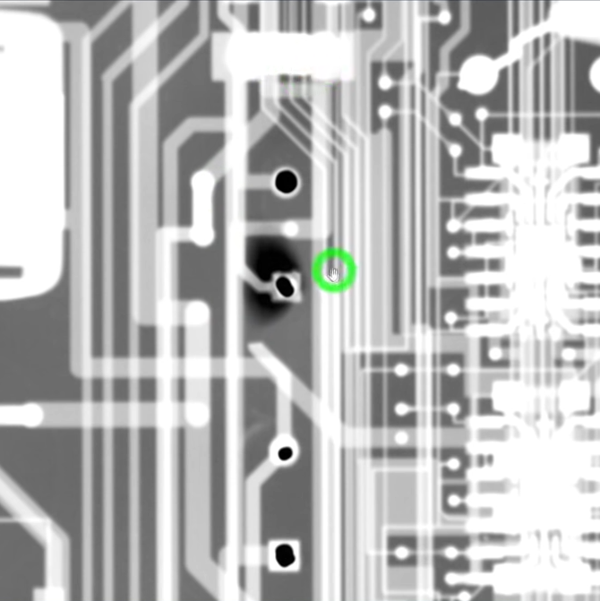
We all know the havoc that water in the wrong place can do to a piece of electronics, and thus we’ve probably all had devices damaged beyond repair. Should [Solderking] have thrown away the water-damaged PCB from a Nintendo Pokemon Ruby cartridge? Of course he should, but when faced with a board on which all vias had succumbed to corrosion he took the less obvious path and repaired them.
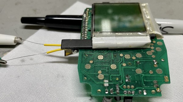
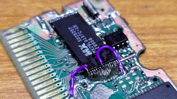
Aside from some very fine soldering in the video below the break there’s little unexpected. He removes the parts and tries a spot of reworking, but the reassembled board doesn’t boot. So he removes them again and this time sands it back to copper. There follows a repair of every single vial on the board, sticking fine wires through the holes into a sponge and soldering the top, before turning it over and fixing the forest of wires on the other side. Fixing the ROM results in a rather challenging fitment involving the chip being mounted at an angle and extra wires going to its pads, which demonstrates the value in this story. It’s not one of monetary value but of persevering with some epic rework to achieve a PCB which eventually boots. Of course a replacement board would make more sense. But that’s not the point, is it?
Continue reading “Fix Every Broken Via To Return This Game To Life”