Integrated Circuits Can Be Easy To Understand With The Right Teachers

For years I’ve been trying to wrap my mind around how silicon chips actually work. How does a purposefully contaminated shard of glass wield control over electrons? Every once in a while, someone comes up with a learning aid that makes these abstract concepts really easy to understand, and this was the case with one of the booths at Maker Faire Bay Area. In addition to the insight it gave me (and hundreds of Faire-goers), here is an example of the best of what Maker Faire stands for. You’ll find a video of their presentation embedded below, along with closeup images of the props used at the booth.

The Uncovering the Silicon booth had a banner and a tablecloth, but was otherwise so unassuming that many people I spoke with missed it. Windell Oskay, Lenore Edman, Eric Schlepfer, John McMaster, and Ken Shirriff took a 50-year-old logic chip and laid it bare for anyone who cared to stop and ask what was on display. The Fairchild μL914 is a dual NOR gate, and it’s age matters because the silicon is not just simple, it’s enormous by today’s standards making it relatively easy to peer inside with tools available to the individual hacker.

ATmega328 decapped by John McMaster was also on display at this booth

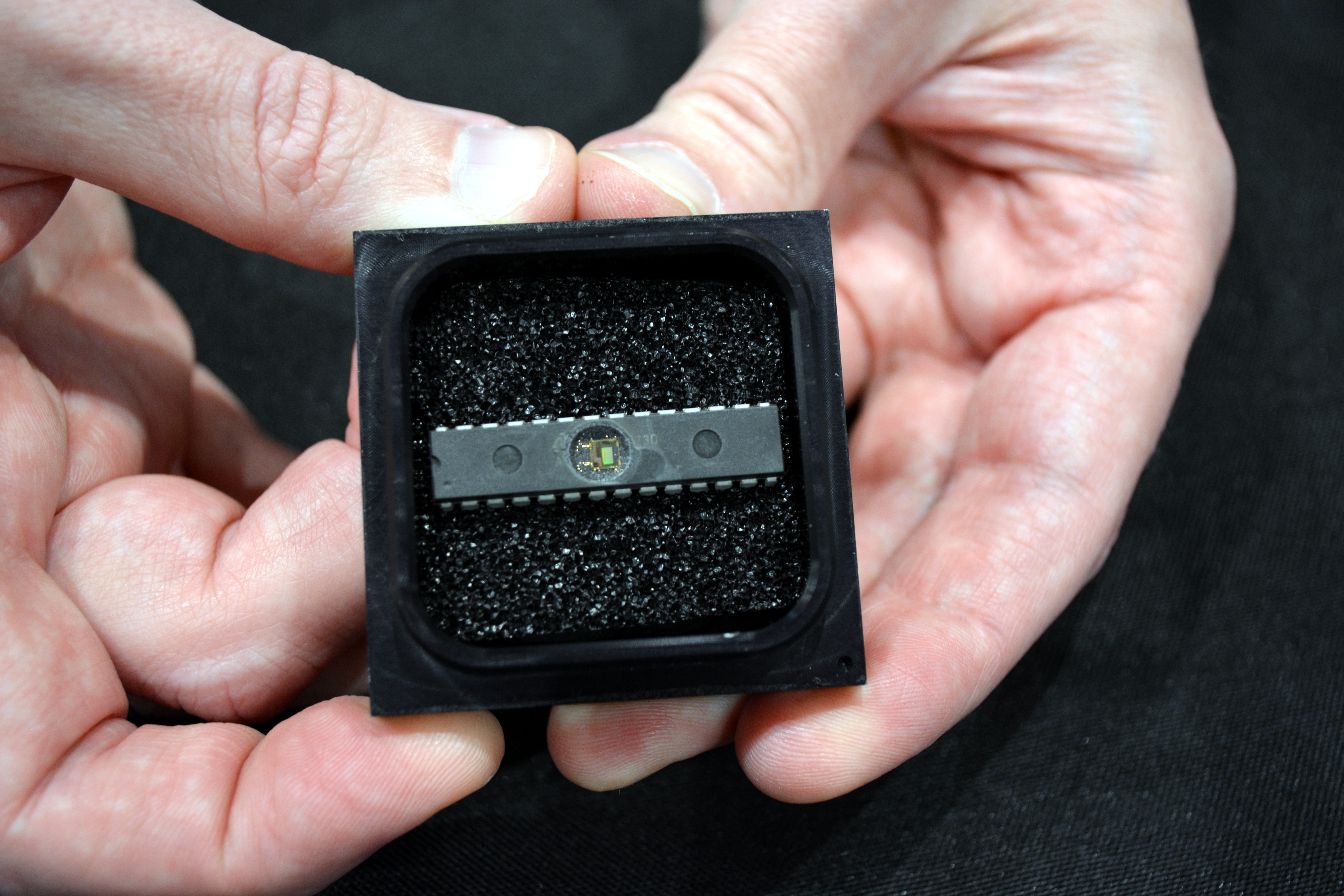
The first challenge is just getting to the die itself. This is John McMaster’s specialty, and you’re likely familiar from his Silicon Pr0n website. He decapped the chip (as well as an ATmega328 which was running the Arduino blink sketch with it’s silicon exposed). Visitors to the booth could look through the microscope and see the circuit for themselves. But looking doesn’t mean understanding, and that’s where this exhibit shines.

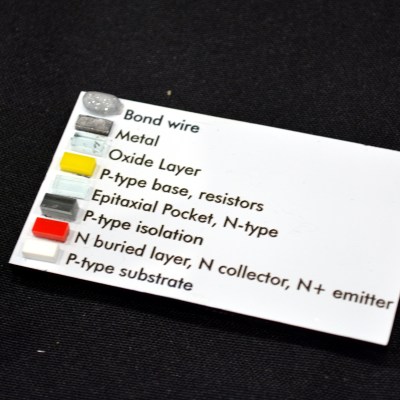
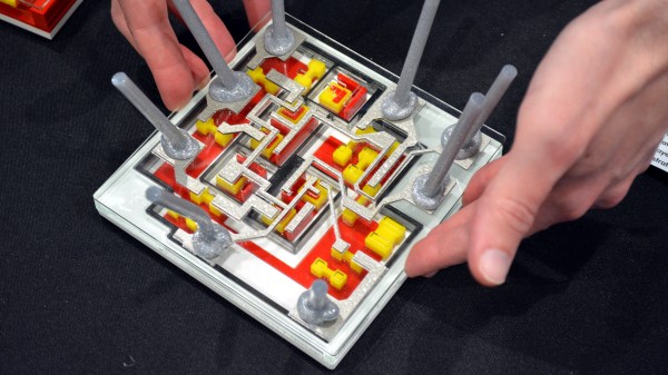
To walk us through how this chip works, a stack-up of laser-cut acrylic demonstrates the base, emitter, and collector of a single transistor. The color coding and shape of this small model makes it easy to pick out the six transistors of the 941 on a full model of the chip. This lets you begin to trace out the function of the circuit.

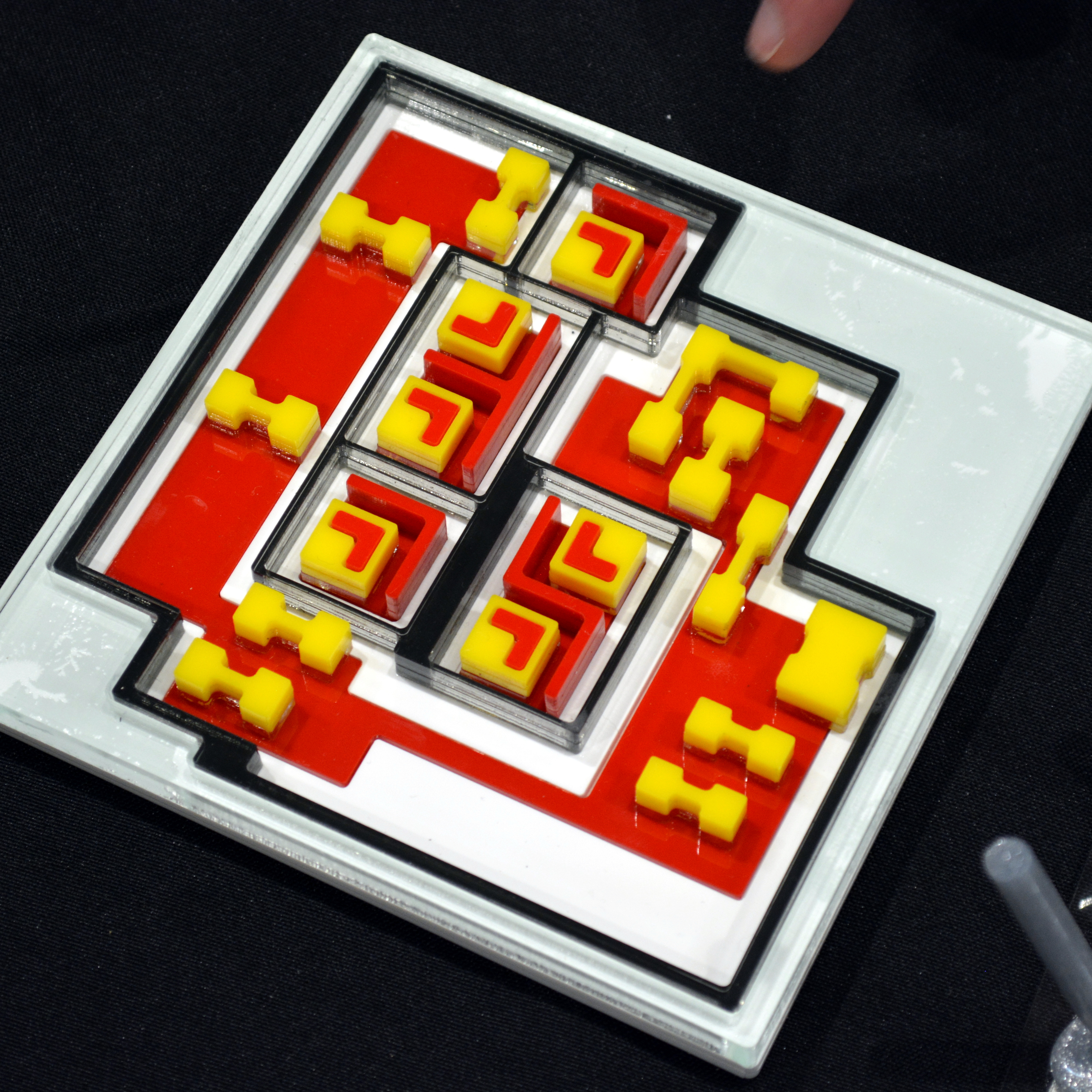
For me, a real ah-ha moment was the resistors in the design. A resistive layer is produced by doping the semiconductor with impurities, making it conduct more poorly. But how do you zero-in on the desired resistance for each part? It’s not by changing the doping, that remains the same. The trick is to make the resistor itself take up a larger footprint. More physical space for the electrons to travel means a lower resistance, and in the model you can see a nice fat resistor in the lower right. The proof for these models was the final showpiece of the exhibit as the artwork of the silicon die was laid out as a circuit board with discrete transistors used to recreate the functionality of the original chip.

Windell takes us through the booth presentation in the video below. I think you’ll be impressed by the breakdown of these concepts and how well they aid in understanding. This was a brilliant concept for an exhibit; it brought together interdisciplinary experts whom I respect and whose work I follow, and sought to invite everyone to gain a better understanding of the secrets hiding in the chips that underpin this technological age. This is exactly the kind of thing I love to see at a Maker Faire.

Continue reading “Integrated Circuits Can Be Easy To Understand With The Right Teachers”

Tiny Art Etched Into Silicon Wafers With Electron Beam Lithography

Looks like [Sam Zeloof] got bored on his Thanksgiving break, and things got a little weird in his garage. Of course when your garage contains a scanning electron microscope, the definition of weird can include experimenting with electron-beam lithography, resulting in tiny images etched into silicon.

You’ll probably remember [Sam] from his 2018 Hackaday Superconference talk on his DIY semiconductor fab lab, which he used to create a real integrated circuit. That chip, a PMOS dual-channel differential amp, was produced by photolithography using a modified DLP projector. Photolithography imposes limits to how small a feature can be created on silicon, based on the wavelength of light.

[Sam] is now looking into using the electron beam of his SEM as a sort of CNC laser engraver to produce much finer features. The process involves spin-coating silicon wafers with SU-8, an epoxy photoresist normally used with UV light but that also turns out to be sensitive to electron beams. He had to modify his SEM to control the X- and Y-axis deflection with a 12-bit DAC and provide a custom beam blanker. With a coated wafer in the vacuum chamber, standard laser engraving software generates the G-code to trace his test images on the resist. A very quick dip in acetone develops the exposed chip.

[Sam] says these first test images are not too dainty; the bears are about 2.5 mm high, and the line width is about 10 μm. His system is currently capable of resolving down to 100 nm, while commercial electron beam lithography can get down to 5 nm or so. He says that adding a Faraday cage to the setup might help him get there. Sounds like a project for Christmas break.

Continue reading “Tiny Art Etched Into Silicon Wafers With Electron Beam Lithography”

Of Roach Killer And Rust Remover: Sam Zeloof’s Garage-Made Chips

A normal life in hacking, if there is such a thing, seems to follow a predictable trajectory, at least in terms of the physical space it occupies. We generally start small, working on a few simple projects on the kitchen table, or if we start young enough, perhaps on a desk in our childhood bedroom. Time passes, our skills increase, and with them the need for space. Soon we’re claiming an unused room or a corner of the basement. Skills build on skills, gear accumulates, and before you know it, the garage is no longer a place for cars but a place for pushing back the darkness of our own ignorance and expanding our horizons into parts unknown.

It appears that Sam Zeloof’s annexation of the family garage occurred fairly early in life, and to a level that’s hard to comprehend. Sam seems to have caught the hacking bug early, and by the time high school rolled around, he was building out a remarkably well-equipped semiconductor fabrication lab at home. Sam has been posting his progress regularly on his own blog and on Twitter, and he dropped by the 2018 Superconference to give everyone a lesson on semiconductor physics and how he became the first hobbyist to produce an integrated circuit using lithographic processes.

Continue reading “Of Roach Killer And Rust Remover: Sam Zeloof’s Garage-Made Chips”

Ken Shirriff Chats About A Whole World Of Chip Decapping

Reverse engineering silicon is a dark art, and when you’re just starting off it’s best to stick to the lesser incantations, curses, and hexes. Hackaday caught up with Ken Shirriff at last year’s Supercon for a chat about the chip decapping and reverse engineering scene. His suggestion is to start with an old friend: the 555 timer.

Ken is well-known for his work photographing the silicon die at the heart of an Integrated Circuit (IC) and mapping out the structures to create a schematic of the circuit. We’re looking forward to Ken’s talk in just a few weeks at the Hackaday Superconference. Get a taste of it in the interview video below.

Continue reading “Ken Shirriff Chats About A Whole World Of Chip Decapping”

Retro-uC, Your Favorite Instruction Sets On Custom Silicon

A few months ago, we caught wind of an interesting project in Big-O Open silicon. It’s a chip, loaded up with the great CPU cores of yore. Now, it’s finally a project on Crowd Supply. The Retro-uC project is an Open Source microcontroller for the retro geek, with a Zilog Z80, MOS 6502, and Motorola 68000 buried in the epoxy of a single QFP package. Oh yes, custom silicon and retro goodness, what more could you want?

The Retro-uC project is part of the Chips4Makers project to develop an Open Source chip for the community. Of course, this has been done before with projects like the HiFive1 and other RISC-V implementations, but really — this is a Z80, 6502 and 68k on a single chip. Let’s not bury the lede here.

As far as the architecture and implementation of these cores go, the ‘active’ core is externally selected on reset, or can be changed through the JTAG interface. There are 72 GPIO pins that can handle 5V, with each pin mapped to the address space of the cores. So far, so good. We can make this work for some really cool stuff.

The JTAG interface is used for testing and programming, although programs can be stored on an external I2C Flash chip and booted from there. There is 4kB of on-chip RAM, and while the peripheral configuration is still being determined, there will at least be UART, I2C, and PWM peripherals. How many of each is anyone’s guess.

The Retro-uC is now a Crowd Supply project, with rewards/orders/whatever ranging from a bare Retro-uC chip for $42 USD to an Arduino Mega-ish development platform for $89, a breadboard version of the chip for $59, and a chip mounted to a Perf2+ prototyping board for $65.

While this chip hasn’t even gotten to tape-out, all the cores work on an FPGA, and there is precedent for doing Open Source, crowdfunded silicon. We’re looking at this one closely and are excited to see what everyone is going to make.

This project has been a long time in the making, with the project lead giving a talk at FOSDEM earlier this year. Now it’s finally time for the hard part of any silicon project — getting the money — and we’re looking forward to see what comes of it.

Robert Hall And The Solid-State Laser

The debt we all owe must be paid someday, and for inventor Robert N. Hall, that debt came due in 2016 at the ripe age of 96. Robert Hall’s passing went all but unnoticed by everyone but his family and a few close colleagues at General Electric’s Schenectady, New York research lab, where Hall spent his remarkable career.

That someone who lives for 96% of a century would outlive most of the people he had ever known is not surprising, but what’s more surprising is that more notice of his life and legacy wasn’t taken. Without his efforts, so many of the tools of modern life that we take for granted would not have come to pass, or would have been delayed. His main contribution started with a simple but seemingly outrageous idea — making a solid-state laser. But he ended up making so many more contributions that it’s worth a look at what he accomplished over his long career.

Continue reading “Robert Hall And The Solid-State Laser”

Fail Of The Week: The Semiconductor Lapping Machine That Can’t Lap Straight

It seemed like a good idea to build a semiconductor lapping machine from an old hard drive. But there’s just something a little off about [electronupdate]’s build, and we think the Hackaday community might be able to pitch in to help.

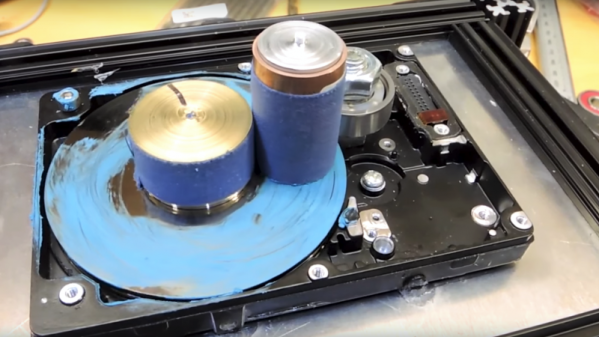
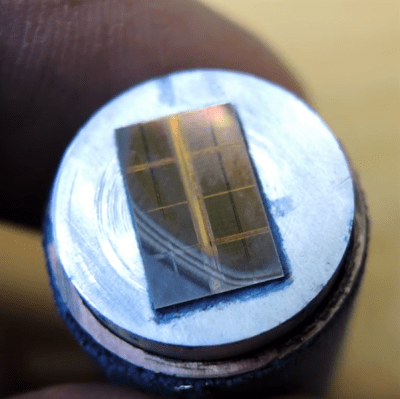
For those not into the anatomy and physiology of semiconductors, getting a look at the inside of the chip can reveal valuable information needed to reverse engineer a device, or it can just scratch the itch of curiosity. Lapping (the gentle grinding away of material) is one way to see the layers that make up the silicon die that lies beneath the epoxy. Hard drives designed to spin at 7200 rpm or more hardly seem a suitable spinning surface for a gentle lapping, but [electronupdate] just wanted the platter for its ultra-smooth, ultra-flat surface.

He removed the heads and replaced the original motor with a gear motor and controller to spin the platter at less than 5 rpm. A small holder for the decapped die was fashioned, and pinched between the platter hub and an idler. It gently rotates the die against the abrasive-covered platter as it slowly revolves. But the die wasn’t abrading evenly. He tried a number of different fixtures for the die, but never got to the degree of precision needed to see through the die layer by layer. We wonder if the weight of the die fixture is deflecting the platter a bit?

Failure is a great way to learn, if you can actually figure out where you went wrong. We look to the Hackaday community for some insight. Check out the video below and sound off in the comments if you’ve got any ideas.

Continue reading “Fail Of The Week: The Semiconductor Lapping Machine That Can’t Lap Straight”