If you were to travel back in time to the turn of the previous century and try to convince the average person that the grains of sand on just about any beach would be the basis of an industry worth hundreds of billions of dollars within 100 years, they’d probably have thought you were crazy. Aside from being coarse, rough, and irritating, sand is everywhere, and convincing anyone of its value would be a hard sell, unless your interlocutor was a real estate visionary with an appreciation of the future value of seaside property and a lot of patience.
Fast forward to our time, and we all know the value of the material that comes from common quartz sand: silicon, specifically the ultra-purified crystals of silicon that end up as the wafers we depend on to build the circuitry of life. The trip from beach to chip foundry is a long and non-obvious one which would not have been possible without the insights of an undistinguished Polish student and one-time druggist who discovered the process that made the Information Age possible: Jan Czochralski.
Chip decapping videos are a staple of the hacking world, and few things compare to the beauty of a silicon die stripped of its protective epoxy and photographed through a good microscope. But the process of actually opening that black resin treasure chest seems elusive, requiring as it does a witch’s brew of solvents and acids.
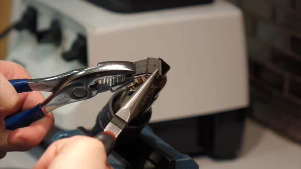
Or does it? As [Curious Marc] documents in the video below, a little heat and some finesse are all it takes, at least for some chips. The method is demonstrated by [Antoine Bercovici], a paleobotanist who sidelines as a collector of old chips. After removing chips from a PCB — he harvested these chips from an old PlayStation — he uses hot air to soften the epoxy, and then flexes the chip with a couple of pairs of pliers. It’s a bit brutal, but in most of the Sony chips he tried for the video, the epoxy broke cleanly over the die and formed a cleavage plane that allowed the die to be slipped out cleanly. The process is not unlike revealing fossils in sedimentary rocks, a process that he’s familiar with from his day job.
He does warn that certain manufacturers, like Motorola and National, use resins that tend to stick to the die more. It’s also clear that a hairdryer doesn’t deliver enough heat; when they switched to a hot air rework station, the success rate went way up.
The simplicity of this method should open the decapping hobby up to more people. Whether you just want to take pretty pictures or if reverse engineering is on your mind, put the white fuming nitric acid down and grab the heat gun instead.
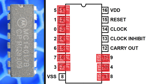
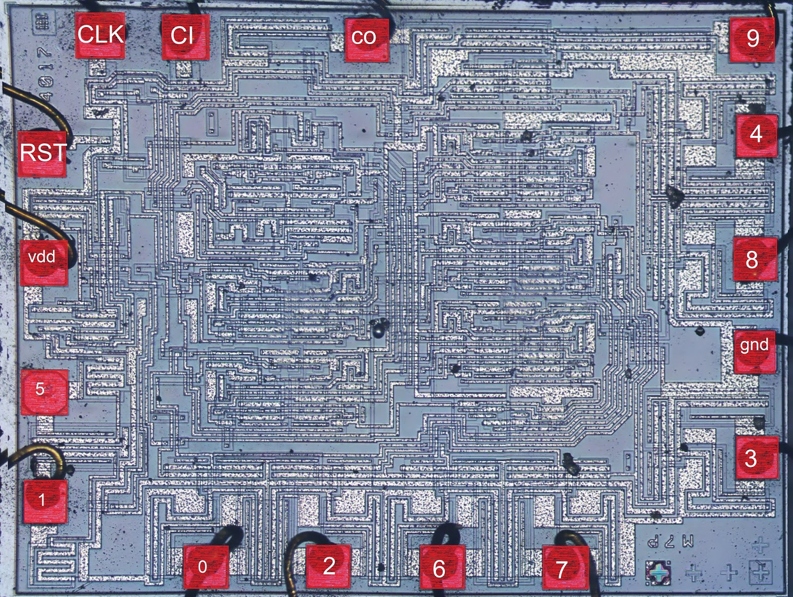
If you’ve ever handled a chip with a really strange or highly inconvenient pinout and suspected that the reason had something to do with the inner workings, you may be interested to see [electronupdate]’s analysis of why the 4017 Decade Counter IC has such a weirdly nonintuitive pinout. It peeks into an IC design dating from the 1970s to see an example of the kind of design issues that can affect physical layout.
In the case of the 4017, once decapped and the inner workings exposed, things became more clear. Inside the chip are a bunch of flip-flops and NAND gates, laid out in a single layer. Some of the outputs (outputs 5 and 1 for example, physically on pins 1 and 2 respectively) share the same flip-flop.
The original design placed the elements in a way that made the most logical sense for routing and layout, which resulted in nice and tidy inner workings but an apparently illogical pinout. A lot of this is probably feeling familiar to anyone who has designed and routed a single-layer PCB, where being limited to one layer makes it important to get the most connections as directly near one another as possible.
Chip design has of course come a long way since the 70s, but there is forever some level of trade-off to be made between outward tidiness and inner design harmony. The next time you’re looking at a part with an apparently illogical pinout, there’s a fair chance it makes far more sense on the inside.
Given the accuracy of Moore’s Law to the development of integrated circuits over the years, one would think that our present day period is no different from the past decades in terms of computer architecture design. However, during the 2017 ACM Turing Award acceptance speech, John L. Hennessy and David A. Patterson described the present as the “golden age of computer architecture”.
Compared to the early days of MS-DOS, when designing user- and kernel-space interactions was still an experiment in the works, it certainly feels like we’re no longer in the infancy of the field. Yet, as the pressure mounts for companies to acquire more computational resources for running expensive machine learning algorithms on massive swaths of data, smart computer architecture design may be just what the industry needs.
Moore’s law predicts the doubling of transistors in an IC, it doesn’t predict the path that IC design will take. When that observation was made in 1965 it was difficult or even impossible to envision where we are today, with tools and processes so closely linked and widely available that the way we conceive processor design is itself multiplying.
After spending much of the 20th century languishing in development hell, electric cars have finally hit the roads in a big way. Automakers are working feverishly to improve range and recharge times to make vehicles more palatable to consumers.
With a strong base of sales and increased uncertainty about the future of fossil fuels, improvements are happening at a rapid pace. Oftentimes, change is gradual, but every so often, a brand new technology promises to bring a step change in performance. Silicon carbide (SiC) semiconductors are just such a technology, and have already begun to revolutionise the industry.
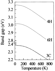
Mind The Bandgap
A graph showing the relationship between band gap and temperature for various phases of Silicon Carbide.
Traditionally, electric vehicles have relied on silicon power transistors in their construction. Having long been the most popular semiconductor material, new technological advances have opened it up to competition. Different semiconductor materials have varying properties that make them better suited for various applications, with silicon carbide being particularly attractive for high-power applications. It all comes down to the bandgap.
Electrons in a semiconductor can sit in one of two energy bands – the valence band, or the conducting band. To jump from the valence band to the conducting band, the electron needs to reach the energy level of the conducting band, jumping the band gap where no electrons can exist. In silicon, the bandgap is around 1-1.5 electron volts (eV), while in silicon carbide, the band gap of the material is on the order of 2.3-3.3 eV. This higher band gap makes the breakdown voltage of silicon carbide parts far higher, as a far stronger electric field is required to overcome the gap. Many contemporary electric cars operate with 400 V batteries, with Porsche equipping their Taycan with an 800 V system. The naturally high breakdown voltage of silicon carbide makes it highly suited to work in these applications.
While most of us are content to buy the chips we need to build our projects, there’s a small group of hackers more interested in making the chips themselves. What it takes the big guys a billion-dollar fab to accomplish, these hobbyists are doing with second-hand equipment, chemicals found in roach killers and rust removers, and a lot of determination to do what no DIYer has done before.
Sam Zeloof is one of this dedicated band, and we’ve been following his progress for years. While he was still in high school, he turned the family garage into a physics lab and turned out his first simple diodes. Later came a MOSFET, and eventually the Z1, a dual-differential amp chip that is the first IC produced by a hobbyist using photolithography.
Sam just completed his first year at Carnegie-Mellon, and he’s agreed to take some precious summer vacation time to host the Hack Chat. Join us as we learn all about the Z1, find out what improvements he’s made to his process, and see what’s next for him both at college and in his own lab.
Click that speech bubble to the right, and you’ll be taken directly to the Hack Chat group on Hackaday.io. You don’t have to wait until Wednesday; join whenever you want and you can see what the community is talking about.
In the hacker and DIY community, there are people who have exceptional knowledge and fantastic tools. These people are able to do what others could only dream about, and that others can only browse eBay looking for that one tool they need to do the job. One of these such people is [John McMaster]. He is the resident expert on looking inside integrated circuits. He drops acid on a chip, and he can tell you exactly how it works on the inside.
At the hardwear.io conference, [John] shared one of his techniques for reverse-engineering intgrated circuits. He’s doing this by simply looking at the transistors, and looking at the light they give off. He’s also looking at the wrong side of the die.
The technique [John] is using is properly called backside analysis, or looking at the infrared emissions of electron recombinations. This happens at the junction of every transistor when it’s active, and these photons are emitted at the bandgap of silicon, or about 1088 nm, far into the infrared. This sort of thing has been done before by [nedos] at CCC in 2013, but rarely have we seen a deep dive into the tools and techniques needed to look at the reverse side of an IC and see the photons coming off.
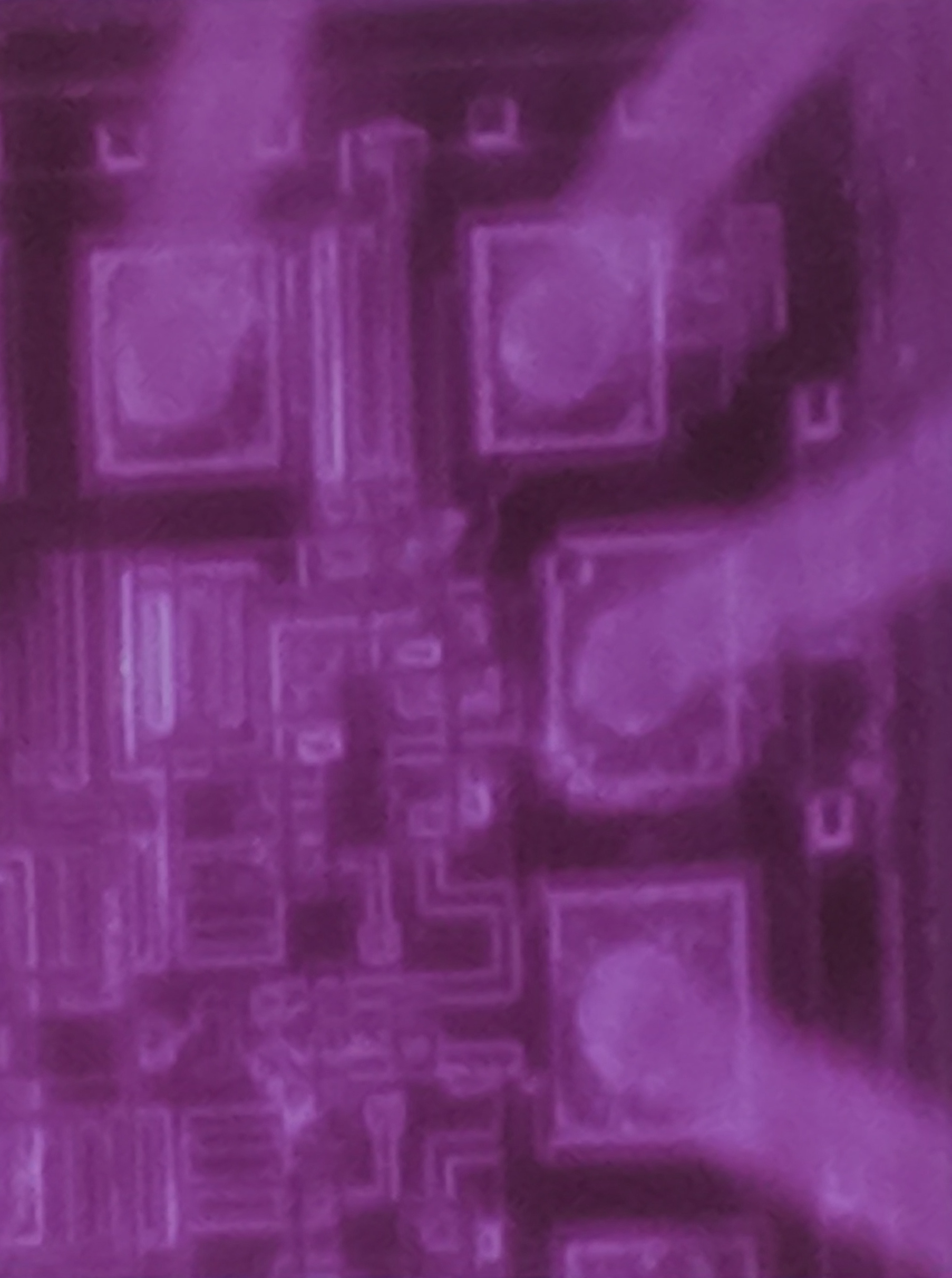
An IC, seen in infrared
There are several tools [John] used for this work, and he actually did a good comparison of different camera technologies used to image infrared photon emissions from integrated circuits. InGaAs cameras are expensive, but they offer high sensitivity. New back-illuminated CMOS cameras and cooled CCDs normally reserved for astrophotography were also tested, and as always, you get what you pay for; the most expensive cameras worked best, but there were ways you could make the cheap ones work.
As with any camera work, preparing the lighting is of utmost importance. This includes an IR pass filter, and using only LED lighting in the lab with no sunlight, incandescent, or halogen light bulbs in the room — you don’t want any IR, after all. A NIR objective in the microscope was sourced from eBay, for about 1/10th the normal cost, because the objective had a small, insignificant scratch. Using this NIR objective made the image twice as bright as any other method. You can successfully image a chip with this, and [John] tested the setup on a resistor inside a CD4050 chip; the resistor glowed a slight purple, the color you would expect with infrared sensors. But can it work with I/O levels in a more modern chip? Also, yes. It needs some Photoshop to process, and stretching the 12-bit or 16-bit color space into an 8-bit color space, but it does work.
Finally, the supreme achievement of doing backside IR analysis. Is that possible with even this minimal setup? This requires some preparation; the silicon substrate in an IC is transparent in IR, but there is attenuation and this is especially important when the substrate is 300 um thick. This needs to be shaved down to about 25 um thick, which surprisingly is best done with fine sandpaper and a finger.
While few IR emissions were observed via backside emissions, the original plan wasn’t to completely analyze the chip, but merely to do some floor planning. For this, it worked. It’s a remarkable amount of work to see the inside of a silicon chip.