Wires Vs Words — PCB Routing In Python

Preferring to spend hours typing code instead of graphically pushing traces around in a PCB layout tool, [James Bowman] over at ExCamera Labs has developed CuFlow, a method for routing PCBs in Python. Whether or not you’re on-board with the concept, you have to admit the results look pretty good.

GD3X Dazzler PCB routed using CuFlow

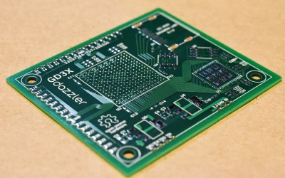
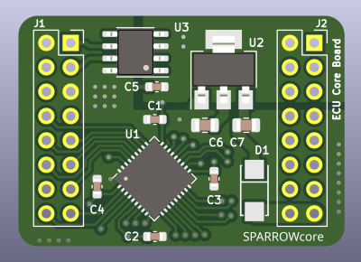
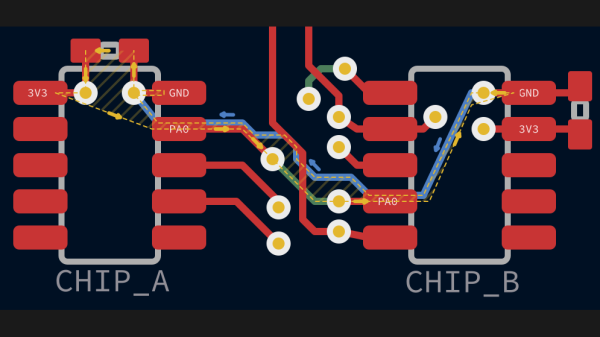
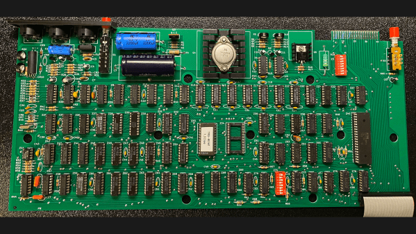
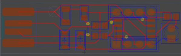
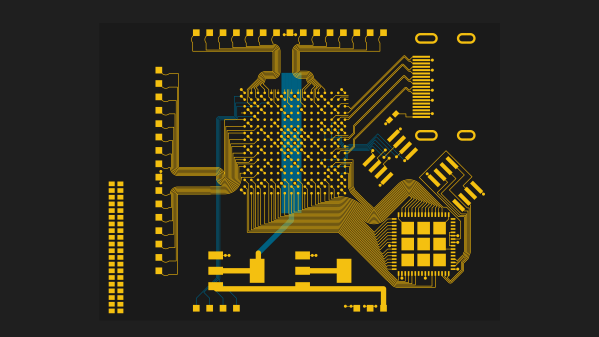
Key to this project is a concept [James] calls rivers — the Dazzler board shown above contains only eight of them. Connections get to their destination by taking one or more of these rivers which can be split, joined, and merged along the way as needed in a very Pythonic manner. River navigation is performed using Turtle graphics-like commands such as left(90) and the appropriately named shimmy(d)that aligns two displaced rivers. He also makes extensive use of pin / gate swapping to make the routing smoother, and there’s a nifty shuffler feature which arbitrarily reorders signals in a crossbar manner. Routing to complex packages, like the BGA shown, is made easier by embedding signal escapes for each part’s library definition.

We completely agree with [James]’s frustration with so many schematics these days being nothing more than a visual net lists, not representing the logical flow and function of the design at all. However, CuFlow further obfuscates the interconnections by burying them deep inside the wire connection details. Perhaps, if CuFlow were melded with something like the SKiDL Python schematic description language, the concept would gain more traction?

That said, we like the concept and routing methodologies he has implemented in CuFlow. Check it out yourself by visiting the GitHub repository, where he writes in more detail about his motivation and various techniques. You may remember [James] two of his embedded systems development tools that we covered back in 2018 — the SPI Driver and the I2C driver.

PCB Design Review: Tinysparrow, A Module For CAN Hacking Needs

I enjoy seeing modules that can make designing other devices easier, and when I did a call for design reviews, [enp6s0] has submitted one such board to us. It’s a module called TinySparrow (GitHub), that helps you build your own vehicle ECUs and any other CAN-enabled things. With a microcontroller, plenty of GPIOs, a linear regulator and a CAN transceiver already onboard, this board has more than enough kick for anyone in hobbyist-range automotive space – and it’s surprisingly tiny!

You could build a lot of things around this module – a CAN bus analyzer or sniffer, a custom peripheral for car dashes, or even a full-blown ECU. You can even design any hardware for a robot or a piece of industrial technology that uses CAN for its backbone – we’ve all seen a few of those! It’s a great board, but it uses six layers. We’ll see if we can do something about that here.

Modules like TinySparrow will make your PCBs cheaper while ordering, too! Thanks to the carefully routed microcontroller and the CAN transmitter, whatever board you design around this chip definitely wouldn’t need six layers like this one does – and, unlike designing your own board, you can use someone’s well-tested and tailored libraries and reference circuits!

With TinySparrow, you save a lot of time, effort and money whenever you want to design a car or industrial accessory. After looking at the board files, my proposal for helping today’s board is – like last time – to make its production cheaper, so that more people can get this board into their hands if the creator ever does try and manufacture it. I also have some tips to make future improvements on this design easier, and make it more friendly for its userbase.

Continue reading “PCB Design Review: Tinysparrow, A Module For CAN Hacking Needs”

Proper Routing Makes For Many Happy Return Paths

Here’s a question for you: when your PCB has a ground plane layer, where do return signals flow? It seems like a trick question, but as [Kristof Mulier] explains, there’s more to return path routing (alternate link in case you run into a paywall) than just doing a copper pour and calling it a day.

Like so many other things in life, the answer to the above question is “it depends,” and as [Kristof] ably demonstrates in this concise article, the return path for a signal largely depends on its frequency. He begins by explaining current loop areas and how they factor into the tendency for a circuit to both emit and be susceptible to electromagnetic noise. The bigger the loop area, the worse things can get from a noise perspective. At low frequencies, return signals will tend to take the shortest possible path, which can result in large current loop areas if you’re not careful. At higher frequencies, though, signals will tend to follow the path of minimal energy instead, which generally ends up being similar to the signal trace, even if it has a huge ground plane to flow through.

Since high-frequency signals naturally follow a path through the ground plane that minimizes the current loop, that means the problem takes care of itself, right? It would, except that we have a habit of putting all kinds of gaps in the way, from ground plane vias to isolation slots. [Kristof] argues that this can result in return paths that wiggle around these features, increasing the current loop area to the point where problems creep in. His solution? Route all your signal return paths. Even if you know that the return traces are going to get incorporated into a pour, the act of intentionally routing them will help minimize the current loop area. It’s brilliantly counterintuitive.

This is the first time we’ve seen the topic of high-frequency return paths tackled. This succinct demonstration shows exactly how return path obstructions can cause unexpected results.

Thanks to [Marius Heier] for the tip.

PCB Design Review: DPI-LVDS Sony Vaio LCD Devboard

Ordering a PCB with mistakes sucks. We should help each other avoid such mistakes – especially newcomers. One of the best ways to avoid these mistakes, especially if it’s your first one, is to get a few other people to look at it. You deserve to get a PCB that is as functional and as helpful as humanly possible, so that you can be happy with your project, and feel ever so slightly more confident in yourself in whatever you shall set out to do next.

At the end of last year, I put out a call for design review submissions, and we’ve received enough projects to make me feel overwhelmed for a bit. A design review has always felt like a personal thing, and here we are doing them in public. But in that sense, we hope that everyone can learn from them, and we hope to push forward a healthy review culture.

What’s more, these articles won’t just be design review. Every project I’m highlighting is worthy of a Hackaday feature just on its own, so tune in and learn more about them!

Today’s Contestant

For this example, I will be walking through a review I’ve already given someone with a pretty cool board, for a pretty cool project I’ve already shown you. Remember the Sony Vaio remake project? A fair bit of people have reached out to me afterwards, and one of them, [Exentio] also had the same Sony Vaio rebuild idea in mind. We started chatting, and he decided to tackle one of the project’s milestones, and perhaps the most crucial one – adapting the LCD.

Continue reading “PCB Design Review: DPI-LVDS Sony Vaio LCD Devboard”

Brand-New PCB Makes Replica TRS-80 Possible

If like us, you missed out on the TRS-80 Model I back when it first came out, relax .With this brand-new PCB that’s a trace-for-trace replica of the original and a bunch of vintage parts, you can build your own from scratch.

Now, obviously, there are easier ways to enjoy the retro goodness that is the 46-year-old machine that in many ways brought the 8-bit hobby computing revolution to the general public’s attention. Sadly, though, original TRS-80s are getting hard to come by, and those that are in decent enough shape to do anything interesting are commanding top dollar. [RetroStack]’s obvious labor of love project provides the foundation upon which to build a brand new TRS-80 as close as possible to the original.

The PCB is revision G and recreates the original in every detail — component layout, connectors, silkscreen, and even trace routing. [RetroStack] even replicated obvious mistakes in the original board, like through-holes that were originally used to fixture the boards for stuffing, and some weird unused vias. There are even wrong components, or at least ones that appear on production assemblies that don’t show up in the schematics. And if you’re going to go through with a build, you’ll want to check out the collection of 3D printable parts that are otherwise unobtainium, such as the bracket for rear panel connectors and miscellaneous keyboard parts.

While we love the devotion to accuracy that [RetroStack] shows with this project, we know that not everyone is of a similar bent. Luckily there are emulators and clones you can build instead. And if you’re wondering why anyone would devote so much effort to half-century-old technology — well, when you know, you know.

Thanks to [Stephen Walters] for the tip.

Feature image: Dave Jones, CC BY-SA 4.0, via Wikimedia Commons


Kicad Autorouting Made Easy

One of the most laborious tasks in PCB layout is the routing. Autorouting isn’t always perfect, but it is nice to have the option, even if you only use it to get started and then hand-tune the resulting board. Unfortunately, recent versions of Kicad have dropped support for autorouting. You can, however, still use Freerouting and the video from [Mr. T] below shows you how to get started.

There are three ways to get the autorouting support. You can install Java and a plugin, you can isntall using a ZIP file, or you can simply export a Specctra DSN file and use Freerouting as a standalone program. Then you import the output DSN file, and you are done.

Continue reading “Kicad Autorouting Made Easy”

Internal Heating Element Makes These PCBs Self-Soldering

Surface mount components have been a game changer for the electronics hobbyist, but doing reflow soldering right requires some way to evenly heat the board. You might need to buy a commercial reflow oven — you can cobble one together from an old toaster oven, after all — but you still need something, because it’s not like a PCB is going to solder itself. Right?

Wrong. At least if you’re [Carl Bugeja], who came up with a clever way to make his PCBs self-soldering. The idea is to use one of the internal layers on a four-layer PCB, which would normally be devoted to a ground plane, as a built-in heating element. Rather than a broad, continuous layer of copper, [Carl] made a long, twisting trace covering the entire area of the PCB. Routing the trace around vias was a bit tricky, but in the end he managed a single trace with a resistance of about 3 ohms.

When connected to a bench power supply, the PCB actually heats up quickly and pretty evenly judging by the IR camera. The quality of the soldering seems very similar to what you’d see from a reflow oven. After soldering, the now-useless heating element is converted into a ground plane for the circuit by breaking off the terminals and soldering on a couple of zero ohm resistors to short the coil to ground.

The whole thing is pretty clever, but there’s more to the story. The circuit [Carl] chose for his first self-soldering board is actually a reflow controller. So once the first board was manually reflowed with a bench supply, it was used to control the reflow process for the rest of the boards in the batch, or any board with a built-in heating element. We expect there will be some limitations on the size of the self-soldering board, though.

We really like this idea, and we’re looking forward to seeing more from [Carl] on this.

Continue reading “Internal Heating Element Makes These PCBs Self-Soldering”