The Ball Grid Array, or BGA package is no longer the exclusive preserve of large, complex chips on computer motherboards: today even simple microcontrollers are available with those little solder balls. Still, many hobbyists prefer to stay with QFP and QFN packages because they’re easier to solder. While that is a fair point, BGA packages can offer significant space savings, and are sometimes the only choice: with the ongoing chip shortage, some other package versions might simply be unavailable. Even soldering doesn’t have to be complicated: if you’re already comfortable with solder paste and reflow profiles, adding a BGA or two into the mix is pretty easy.
In this article we’ll show that working with BGA chips is not as difficult as it may seem. The focus will be on printed circuit board design: how to draw proper footprints, how to route lots of signals and what capabilities your PCB manufacturer should have. We’ll cover soldering and rework techniques in a future article, but first let’s take a look at why BGAs are used at all.
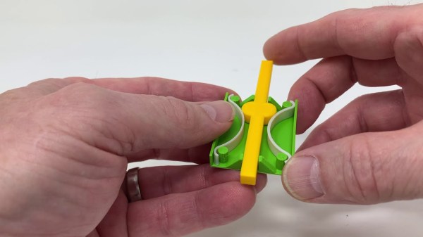
Plastics are wonderous materials, much loved for their ability to elastically deform and spring back to their original shape. They’re a category of materials perfect for creating things like living hinges and similar mechanisms, and this 3D printed snap action device shows that off admirably.
The device consists of an outer housing, into which two printed springs are inserted. These leaf springs are curved and protrude towards the center of the housing. A slide is then inserted into the housing with a cam in its middle. The cam allows the slide to push past the springs when actuated, while also holding it in place at rest.
As demonstrated the mechanism reliably snaps back and forth between its two positions in a satisfying manner. It’s shown with one side of the housing removed so we get a good idea of how it works. It’s 100% 3D printed, as well. Anyone looking to replicate the design should note the importance of printing orientation, particularly in the case of the spring pieces, which won’t work if layered up in the wrong way.
Overall, it’s a neat design that could prove useful for those eager to build printed switches or other mechanical devices. It’s also simply a great way to learn about 3D printed springs and working with deformable plastic structures. Video after the break.
Buying broken gear for cheap is time honored hacker tradition, and while we might not always be successful in reviving it, rarely do we come away empty handed. There’s always parts to salvage, and you can’t put a price on the knowledge to be gained when poking around inside an interesting piece of hardware. So we’re not surprised at all to hear that [Tomas Pavlovic] jumped at the chance to grab this faulty HP-48S calculator for a couple bucks.
Luckily for us, the story doesn’t end at the bottom of his parts bin. When he got the HP-48S back home, he immediately set out to see if it could be repaired. After changing out a few choice components and not seeing any result in the device’s behavior, he became suspicious that the problem may be with the firmware; specifically, the soldered-on chip that holds it.
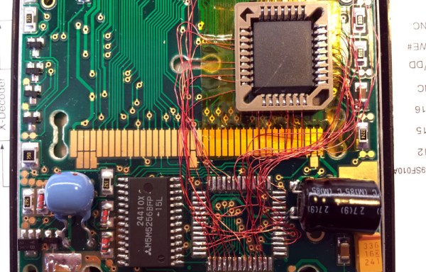
Dumping the original ROM.
After carefully lifting the NEC uPD23C2000GC from its resting place for the last 30 years or so, he wired up an adapter that let him connect the chip to his programmer so its contents could be dumped. Rather than trying to find another ROM chip, he decided to wire in a socket and found a re-writable SST39SF040 that could stand in as a replacement. Flashing a fresh copy of the firmware to the new socketed chip got the calculator up and running again, with the added bonus of allowing [Tomas] to pull the chip and flash a different firmware version should he care to experiment a bit.
Now, we know what you’re thinking. Where was the fix? What exactly brought this piece of 1990s gear back to life? That part, unfortunately, isn’t very clear. You’d think if the original ROM chip was somehow faulty, [Tomas] wouldn’t have been able to so easily pull a valid firmware image from it. That leaves us with some pretty mundane possibilities, such as a bad solder joint on the chip’s pins. If that was indeed the case, this fix could have been as simple as running a hot iron over the pins…but of course, where’s the fun in that?
Update: We heard back from [Tomas], and it turns out that when compared to a known good copy, the dumped firmware did have a few swapped bits. His theory is that the NEC chip is in some weird failure mode where the calculator wouldn’t run, but it was still functional enough to get most of the content off of it. What do you think? Let us know in the comments.
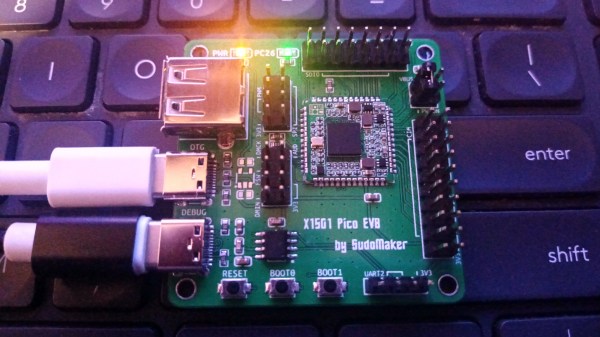
Ever wanted to run Linux in an exceptionally small footprint? Then [Reimu NotMoe] from [SudoMaker] has something for you! She’s found an unbelievably small Linux-able chip in BGA, and designed a self-contained tiny SoM (System on Module) breakout with power management and castellated pads. This breakout contains everything you need to have Linux in a 16x16x2mm footprint. For the reference, a 16mm square is the size of the CPU on a Raspberry Pi.
This board isn’t just tiny, it’s also well-thought-out, helping you put the BGA-packaged Ingenic X1501 anywhere with minimal effort. With castellated pads, it’s easy to hand-solder this SoM for development and reflow for production. An onboard switching regulator works from 6V down to as low as 3V, making this a viable battery-powered Linux option. It can even give you up to 3.3V/1A for all your external devices.
The coolest part yet – the X1501 is surprisingly friendly and NDA-free. The datasheets are up for grabs, there are no “CONFIDENTIAL” watermarks – you get a proper 730-page PDF. Thanks to this openness, the X1501 can run mainline Linux with minimal changes, with most of the peripherals already supported. Plus, there’s Efuse-based Secure Boot if your software needs to be protected from cloning.
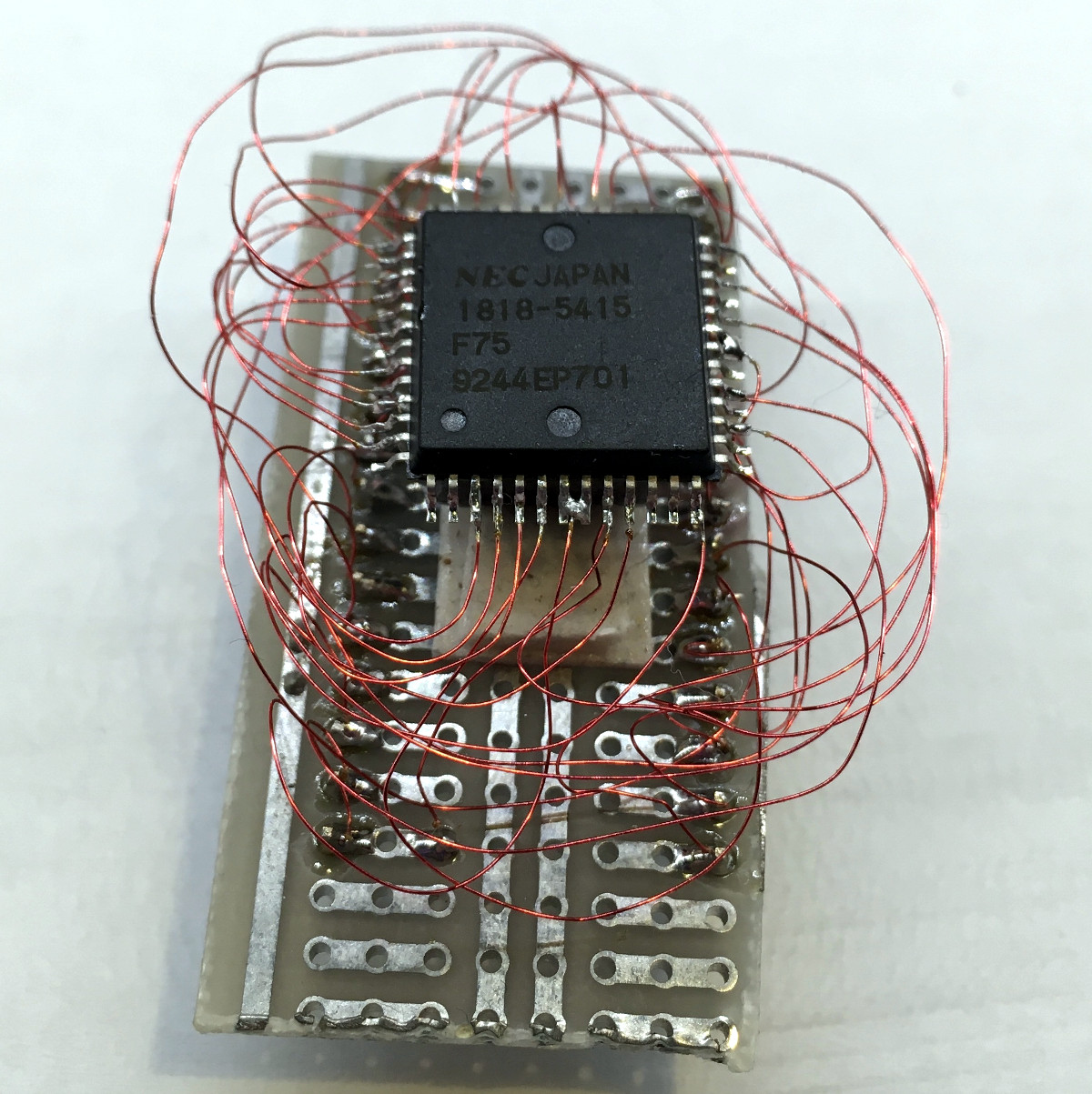
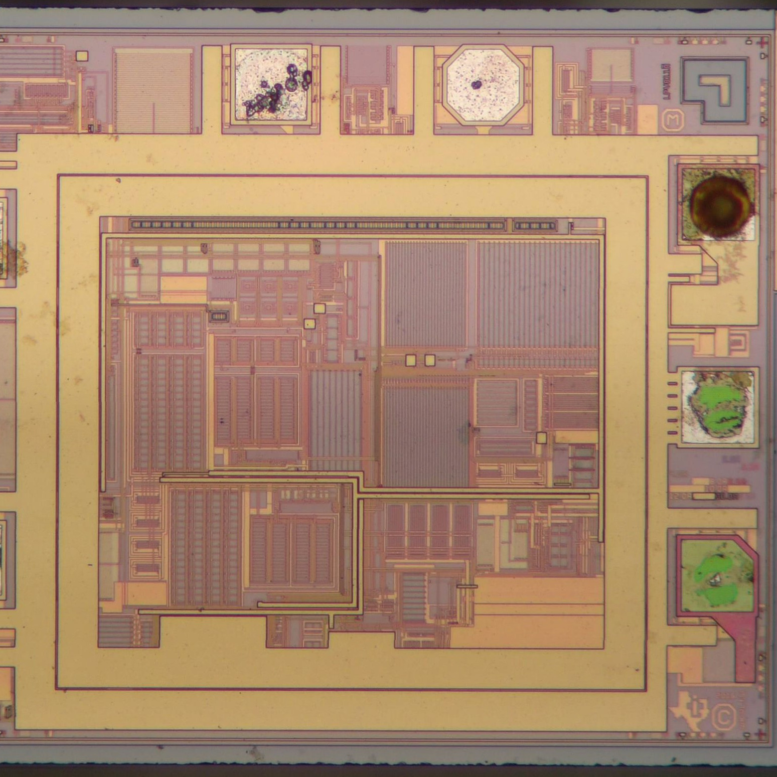
[Robo] over at Tiny Transistor Labs has a fascinating look at what’s inside these modern, ultra low-power devices that consume absolutely minuscule amounts of current. Crank up the magnification, and go take a look at the dies on these two similar (but internally very different) devices.
Texas Instruments LPV801, under the hood.
The first unit is the Texas Instruments LPV801, a single-channel op-amp that might not be very fast, but makes up for it by consuming only a few hundred nanoamps. Inside, [Robo] points out all the elements of the design, explaining how a part like this would be laser-trimmed to ensure it performs within specifications.
The second part is the Texas Instruments LPV821 which uses a wee bit more power, but makes up for it with a few extra features like zero-drift and EMI hardening. Peeking inside this device reveals the different manufacturing process this part used, and [Robo] points out things like the apparent lack of fuses for precise trimming of the part during the manufacturing process.
Seeing these structures up close isn’t an everyday thing for most of us, so take the opportunity to check out [Robo]’s photos. Tiny Transistor Labs definitely takes the “tiny” part of their name seriously, as we’ve seen with their 555 timer, recreated with discrete transistors, all crammed into a package that’s even the same basic size as the original.
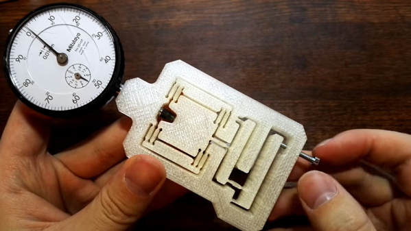
Here’s an older but fantastic video that is as edifying as it is short. [Topias Korpi] demonstrates a 3D printed flexure with a dial indicator on one end, and an M3 screw on the other. As the screw is turned, the dial indicator moves steadily with roughly a 15:1 reduction between the movement of the screw and the indicator. Stable deflections of 0.01 mm are easily dialed in, and it’s neat seeing it work while the flexure itself shows no perceptible movement. A demonstration is embedded below the page break and is less than a minute long, so give it a watch and maybe get some ideas.
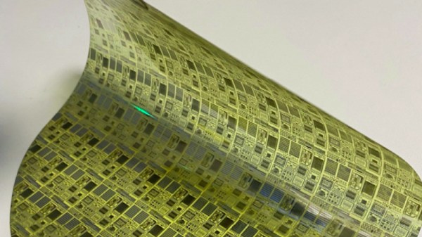
While our attention is mostly directed towards ever smaller-integrated silicon circuits providing faster and faster computing, there’s another area of integrated electronics that operates at a much lower speed which we should be following. Thin-film flexible circuitry will provide novel ways to place electronics where a bulky or expensive circuit board with traditional components might be too expensive or inappropriate, and Wikichip is here to remind us of a Leuven university team who’ve created what is claimed to be the fastest thin-film flexible microprocessor yet. Some of you might find it familiar, it’s our old friend the 6502.
The choice of an archaic 8-bit processor might seem a strange one, but we can see the publicity advantage — after all, you’re reading about it here because of it being a 6502. Plus there’s the advantage of it being a relatively simple and well-understood architecture. It’s no match for the MHz clock speeds of the original with an upper limit of 71.4 kHz, but performance is not the most significant feature of flexible electronics. The production technology isn’t quite ready for the mainstream so we’re unlikely to be featuring flexible Commodore 64s any time soon, but the achievement is the impressive feat of a working thin-film flexible microprocessor.