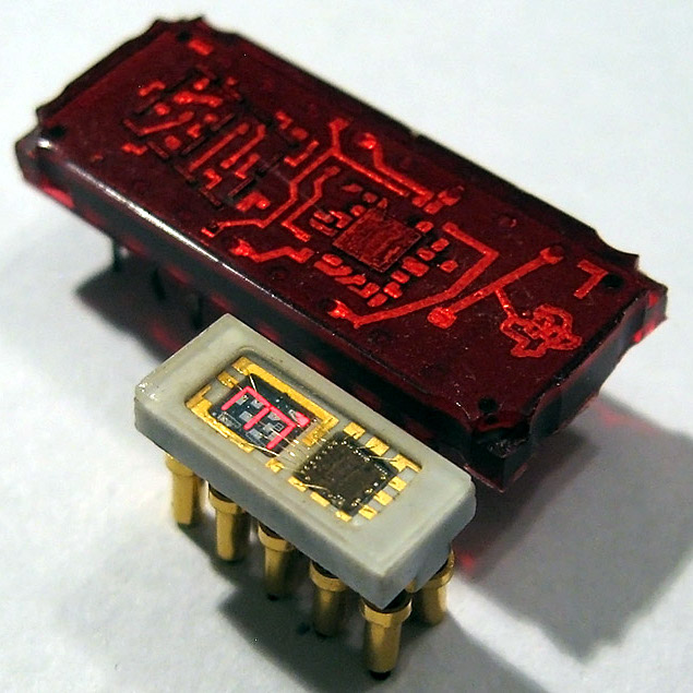
For most of human history, our inventions and innovations have been at a scale that’s literally easy to grasp. From the largest cathedral to the finest pocket watch, everything that went into our constructions has been something we could see with our own eyes and manipulate with our hands. But in the middle of the 20th century, we started making really, really small stuff: semiconductors. For the first time, we were able to create mechanisms too small to be seen with the naked eye, and too fine to handle with our comparatively huge hands. We needed a way to scale these devices up somewhat to make them useful parts. In short, they needed to be packaged.
We know that the first commercially important integrated circuits were packaged in the now-familiar dual in-line package (DIP), the little black plastic millipedes that would crawl across circuit boards for the next 50 years. As useful and versatile as the DIP was, and for as successful as the package became, its design was anything but obvious. Let’s take a look at the dual in-line package and how it got that way.
Continue reading “The Dual In-Line Package And How It Got That Way”
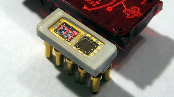
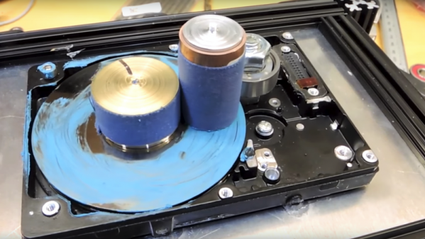
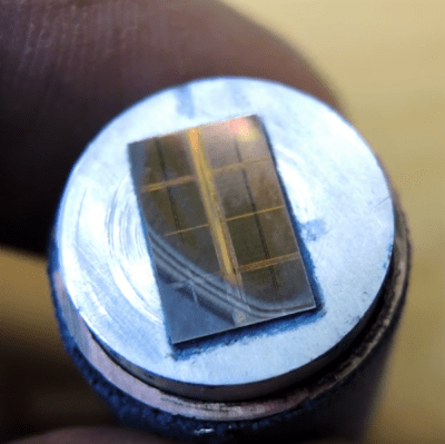 For those not into the anatomy and physiology of semiconductors, getting a look at the inside of the chip can reveal valuable information needed to reverse engineer a device, or it can just scratch the itch of curiosity. Lapping (the gentle grinding away of material) is one way to see the layers that make up the silicon die that lies beneath the epoxy. Hard drives designed to spin at 7200 rpm or more hardly seem a suitable spinning surface for a gentle lapping, but [electronupdate] just wanted the platter for its ultra-smooth, ultra-flat surface.