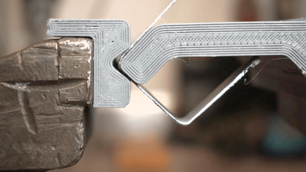
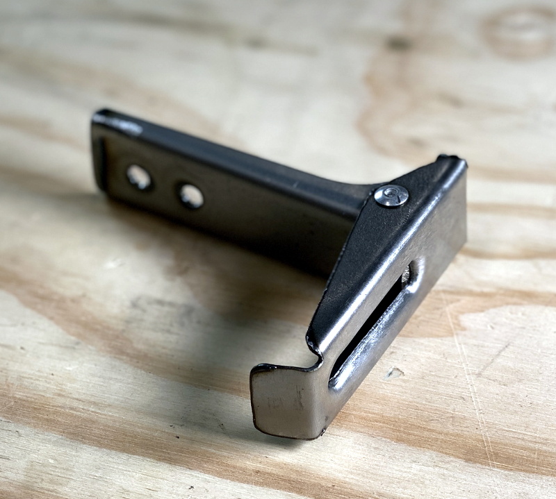
Using 3D printed forms to bend sheet metal isn’t exactly new. We’ve seen several people create custom dies for their brakes, and the results have shown the concept has merit for small-scale production. But that’s usually where the process ends. A bend here or there is one thing, but the ability to form a complex shape with them has always seemed like asking too much. But judging by his recent experiments, [Shane Wighton] is very close to changing that perception.
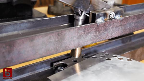
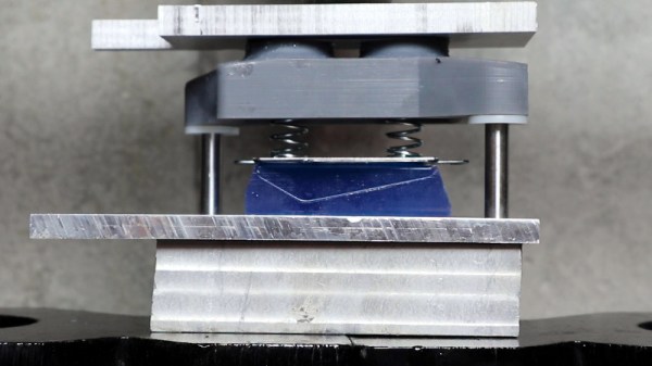
 The process at work here is, relatively speaking, pretty simple. You print out the upper and lower die, put a piece of sheet metal between them, and then smash them together with a hydraulic press. If everything works correctly, and your CAD skills hold true, the metal will take the desired shape.
Of course, that’s vastly oversimplifying things. As [Shane] explains in the video after the break, there are many nuances to forming sheet metal like this that need to be taken into account, and iteration and experimentation are basically unavoidable. So it’s a good thing you can rapidly redesign and reprint the dies.
Which isn’t to say that the dies themselves didn’t come with their own unique set of challenges. The first ones shattered under the pressure, and it took a few design revisions and eventually a switch to a stronger resin before [Shane] got a set of dies that could form the desired piece. Even still, he’s had a lot of trouble getting the printed parts to survive multiple uses. But he’s confident with some more refinements he could get a repeatable process going, and thinks ultimately producing runs of up to 100 parts on a set of printed dies isn’t out of the question.
Logically, it would seem plastic isn’t an ideal choice for punching and shaping metal. Frankly, it’s not. But if you’re doing in-house manufacturing, the ability to produce complex tooling quickly and easily can help make up for any downsides it might have.
Continue reading “Forming Sheet Metal Parts With 3D Printed Dies”