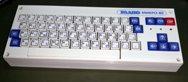
[Alex Zaikin] made a modern reproduction of an early-80s Soviet hobbyist home computer. Although the design was open, indeed it was published in “Radio” magazine, the project was a mammoth undertaking involving around 200 microchips, so not many “Mikro-80” computers were actually made.
[Alex] wanted to simplify the project and reduce the parts count. These days, 200 microchips’ worth of logic can easily fit inside an FPGA, and [Alex] wrangled the chip count down to seven. Moreover, he made it even easier to build your own retro minicomputer by building a modular platform: Retrobyte.
With the Retrobyte providing all of the essential infrastructure — SD card, tape recorder I/O, VGA outputs, and more — and the FPGA providing the brains, all that was left was to design a period keyboard and 3D print a nice enclosure. Project complete! Time for a few rounds of ASCII Tetris to celebrate.
We’ve covered a number of retro computer projects. We just have a soft spot for them, is all. If you don’t know what all the fuss is about, you could start out with a kit build to get your feet wet. Before long, you’ll be emulating ever obscurer computers of yore in custom logic. And when you do, be sure to drop us a line!
A few years ago, [Kingpin] a.k.a. [Joe Grand] (A judge for the 2014 Hackaday Prize) designed the most beautiful electronic prank ever. The BSODomizer is a simple device with a pass-through connection for a VGA display and an infrared receiver. Plug the BSODomizer into an unsuspecting coworker’s monitor, press a button on a remote, and watch Microsoft’s blue screen of death appear. It’s brilliant, devious, and actually a pretty simple device if you pick the right microcontroller.
The original BSODomizer is getting a little long in the tooth. VGA is finally dead. The Propeller chip used to generate the video only generates text, and can’t reproduce Microsoft’s fancy new graphical error screens. HDMI is the future, and FPGAs have never been more accessible. For this year’s DEF CON, [Kingpin] and [Zoz] needed something to impress an audience that is just learning how to solder. They’ve revisited the BSODomizer, and have created the greatest hardware project at this year’s DEF CON.
Playing around with FPGAs used to be a daunting prospect. You had to fork out a hundred bucks or so for a development kit, sign the Devil’s bargain to get your hands on a toolchain, and only then can you start learning. In the last few years, a number of forces have converged to bring the FPGA experience within the reach of even the cheapest and most principled open-source hacker.
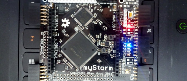
[Ken Boak] and [Alan Wood] put together a no-nonsense FPGA board with the goal of getting the price under $30. They basically took a Lattice iCE40HX4K, an STMF103 ARM Cortex-M3 microcontroller, some SRAM, and put it all together on a single board.
The Lattice part is a natural choice because the IceStorm project created a full open-source toolchain for it. (Watch [Clifford Wolf]’s presentation). The ARM chip is there to load the bitstream into the FPGA on boot up, and also brings USB connectivity, ADC pins, and other peripherals into the mix. There’s enough RAM on board to get a lot done, and between the ARM and FPGA, there’s more GPIO pins than we can count.
Modeling an open processor core? Sure. High-speed digital signal capture? Why not. It even connects to a Raspberry Pi, so you could use the whole affair as a high-speed peripheral. With so much flexibility, there’s very little that you couldn’t do with this thing. The trick is going to be taming the beast. And that’s where you come in.
[Lukas] started his epic SDR-from-scratch build when he was 16. Projects like this aren’t completed overnight. (He’s now 18. We’re impressed.)
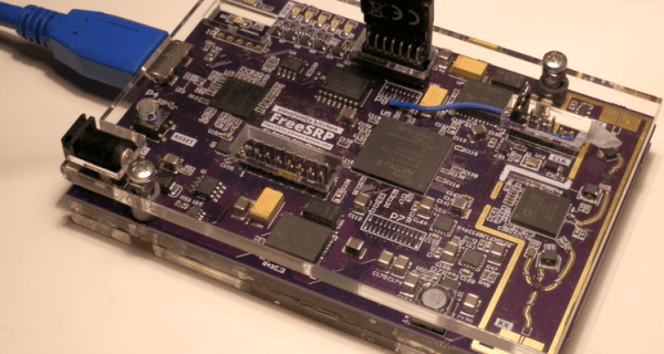
The project itself is a Software-Defined Radio built on top of the 12-bit Analog Devices AD9364 transceiver IC. A big fat FPGA takes the data and runs it off to a USB 3.0 interface, which is necessary for the amount of data this thing will be producing — he’s got it receiving 56 MHz of bandwidth. In short, this is an SDR peripheral that’s in the big leagues.
After two years of work and (only!) three revision, [Lukas] got the thing working. Read his writeup for the blow-by-blow account. In the end, a 6-layer board was necessary for the routing to get the full speed out of the clocking, and he discovered the reason that you use exactly the specified bias resistors — the expensive ADC chip gets very hot. But he didn’t give up, and in the end he pulled off a project of immense complexity. In his own words:
I have discovered that taking on large projects, even when not knowing how to tackle problems that might arise, is a very effective way of learning for me. It’s just important to be persistent, as I’ve seen that almost any problem can be solved on your own — which is incredibly rewarding — even if you get stuck and seem to not make progress for a while.
[Lukas] is now working on the software. He’s already got a hacked osmocom driver working, so it plays nice with GNURadio.
Of course, there are tons of ways to get into SDR without building your own from scratch, but we applaud [Lukas] for going the hard way. If you’re tempted to follow in his footsteps, have a look at [Michael Ossmann]’s great talk on making the RF design process as tractable as possible.
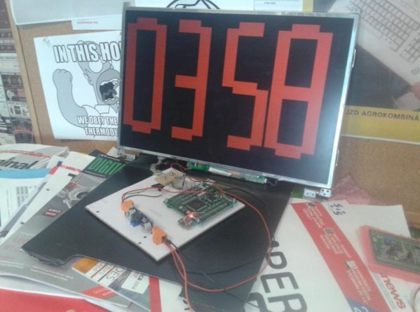
Every year, new models of laptops arrive on the shelves. This means that old laptops usually end up in landfills, which isn’t exactly ideal. If you don’t want to waste an old or obsolete laptop, though, there’s a way to reuse at least the screen out of one. Simply grab an FPGA off the shelf and get to work.
[Martin] shows us all how to perform this feat on our own, and goes into great detail about how all of the electronics involved work. Once everything was disassembled and the FPGA was wired up, it took him a substantial amount of time just to turn the display on. From there it was all downhill: [Martin] can now get any pattern to show up on the screen, within reason. The only limit to his display now seems to be the lack of external RAM. He currently uses the setup to drive an impressive-looking clock.
This is a big step from days passed where it was next to impossible to repurpose a laptop screen. Eventually someone discovered a way to drive these displays, and now there are cheap electronics from China that can usually get a screen like this running. It’s impressive to see it done from scratch, though, and the amount of detail in the videos are a great way to understand how everything is working.
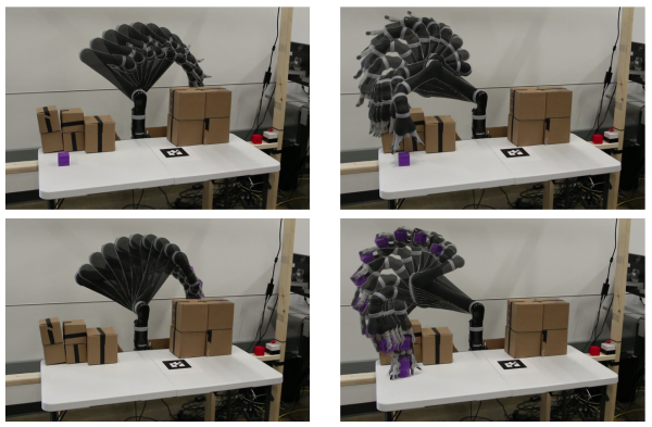
For humans, moving our arms and hands onto an object to pick it up is pretty easy; but for manipulators, it’s a different story. Once we’ve found the object we want our robot to pick up, we still need to plan a path from our robot hand to the object all the while lugging the remaining limbs along for the ride without snagging them on any incoming obstacles. The space of all possible joint configurations is called the “joint configuration space.” Planning a collision-free path through them is called path planning, and it’s a tricky one to solve quickly in the world of robotics.
These days, roboticists have nailed out a few algorithms, but executing them takes 100s of milliseconds to compute. The result? Robots spend most of their time “thinking” about moving, rather than executing the actual move.
Robots have been lurching along pretty slowly for a while until recently when researchers at Duke University [PDF] pushed much of the computation to hardware on an FPGA. The result? Path planning in hardware with a 6-degree-of-freedom arm takes under a millisecond to compute!
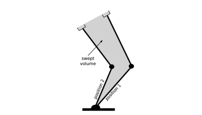
It’s worth asking: why is this problem so hard? How did hardware make it faster? There’s a few layers here, but it’s worth investigating the big ones. Planning a path from point A to point B usually happens probabilistically (randomly iterating to the finishing point), and if there exists a path, the algorithm will find it. The issue, however, arises when we need to lug our remaining limbs through the space to reach that object. This feature is called the swept volume, and it’s the entire shape that our ‘bot limbs envelope while getting from A to B. This is not just a collision-free path for the hand, but for the entire set of joints.
Image Credit: Robot Motion Planning on a Chip
Encoding a map on a computer is done by discretizing the space into a sufficient resolution of 3D voxels. If a voxel is occupied by an obstacle, it gets one state. If it’s not occupied, it gets another. To compute whether or not a path is OK, a set of voxels that represent the swept volume needs to be compared against the voxels that represent the environment. Here’s where the FPGA kicks in with the speed bump. With the hardware implementation, voxel occupation is encoded in bits, and the entire volume calculation is done in parallel. Nifty to have custom hardware for this, right?
We applaud the folks at Duke University for getting this up-and-running, and we can’t wait to see custom “robot path-planning chips” hit the market some day. For now, though, if you’d like to sink your teeth into seeing how FPGAs can parallelize conventional algorithms, check out our linear-time sorting feature from a few months back.
[Bunnie Huang] and [Edward Snowden] have teamed up to publish a paper exploring the possibility of introspection on the iPhone.
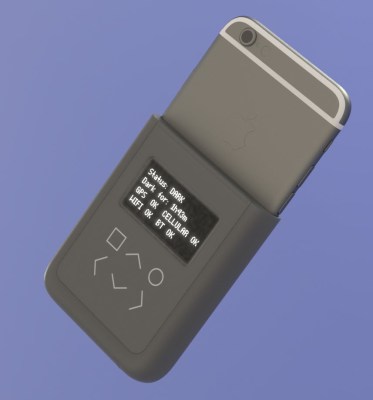
A rendering of the proposed introspection device attached to an iPhone6
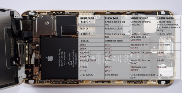
The idea is that phones are increasingly complex and potentially vulnerable to all kinds of digital surveillance. Even airplane mode is insufficient for knowing that your phone isn’t somehow transmitting information. The paper looks at the various radios on the iPhone, going so far as opening up the device and reading signals at each of the chips for cell, WiFi, Bluetooth, GPS, and NFC to determine whether the chip itself is doing anything, regardless of what the screen says. This introspection can then be used to be confident that the phone is not communicating when it shouldn’t be.
The paper goes on to propose a device that they will prototype in the coming year which uses an FPC that goes into the phone through the SIM card port. It would contain a battery, display, buttons, multiple SIM cards, and an FPGA to monitor the various buses and chips and report on activity.
Significant hacking of an iPhone will still be required, but the idea is to increase transparency and be certain that your device is only doing what you want it to.