Fail Of The Week: PCB LED Cube Fails Successfully

Remember LED cubes? We sure do — they were all the rage for a while, and then it seemed like everyone just sort of lost interest in them. There are probably a lot of reasons for that, not least of which is likely the amount of work it takes to put one together from discrete LEDs and separate pieces of wire. Could there be a better way?

Of course there could, and [Sasa Karanovic] thought he had it all figured out with this PCB-based LED cube. At first glance, it seems to make perfect sense; after all, weren’t PCBs invented to take the place of all that pesky point-to-point wiring in the early days of electronics? The boards [Sasa] designed are pretty cool, actually. They’ve each got room for 16 addressable WS2812 LEDs in 5 mm packages, with every possible bit of substrate removed to block the minimum amount of light. That left very little room for traces on the 2-mm-wide arms, so the PCBs had to have four layers, which raised eyebrows at the PCB house when [Sasa] submitted the design.

Such an airy and open design obviously has the potential for mechanical issues, which [Sasa] addressed by adding pads at three corners of each board; a vertical PCB connects to each LED board to provide mechanical support and distribute signals to the LEDs. The cube seems solid enough as a result, and even when handled the LED boards don’t really flop around too much. See the cube in action in the video below.

What’s nice about this design is the perfect spacing between the LEDs in all three dimensions, and the way everything lines up nice and straight. That would be really hard to do with wire, even for the most practiced of circuit sculptors. [Sasa] seems to agree, but still deems the build a failure because the PCBs block too much of the view. We suppose he’s got a point, and we’re not sure how well this would scale to an 8×8 cube. We’re not sure how we’d feel about paying for PCBs that are mostly air either, but as failures go, this one still manages to be pretty successful. Continue reading “Fail Of The Week: PCB LED Cube Fails Successfully”

Brand-New PCB Makes Replica TRS-80 Possible

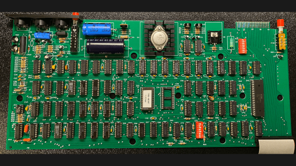
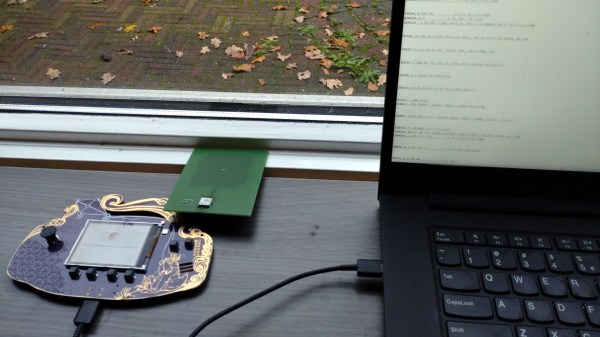
If like us, you missed out on the TRS-80 Model I back when it first came out, relax .With this brand-new PCB that’s a trace-for-trace replica of the original and a bunch of vintage parts, you can build your own from scratch.

Now, obviously, there are easier ways to enjoy the retro goodness that is the 46-year-old machine that in many ways brought the 8-bit hobby computing revolution to the general public’s attention. Sadly, though, original TRS-80s are getting hard to come by, and those that are in decent enough shape to do anything interesting are commanding top dollar. [RetroStack]’s obvious labor of love project provides the foundation upon which to build a brand new TRS-80 as close as possible to the original.

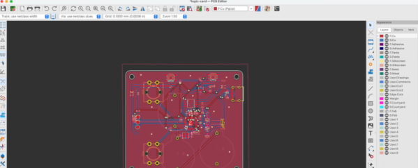
The PCB is revision G and recreates the original in every detail — component layout, connectors, silkscreen, and even trace routing. [RetroStack] even replicated obvious mistakes in the original board, like through-holes that were originally used to fixture the boards for stuffing, and some weird unused vias. There are even wrong components, or at least ones that appear on production assemblies that don’t show up in the schematics. And if you’re going to go through with a build, you’ll want to check out the collection of 3D printable parts that are otherwise unobtainium, such as the bracket for rear panel connectors and miscellaneous keyboard parts.

While we love the devotion to accuracy that [RetroStack] shows with this project, we know that not everyone is of a similar bent. Luckily there are emulators and clones you can build instead. And if you’re wondering why anyone would devote so much effort to half-century-old technology — well, when you know, you know.

Thanks to [Stephen Walters] for the tip.

Feature image: Dave Jones, CC BY-SA 4.0, via Wikimedia Commons


Raspberry Pi 5 Goes Under The X-ray

Most Hackaday readers will know to some extent what lies inside their computer, even if this is only at a block diagram level listing the peripherals. But what is physically on a modern computer board? [Jeff Geerling] has subjected a Raspberry Pi 5 to a medical imager, and shares with us the many layers of parts and PCB he found there. With a six-layer board and a heap of large BGA chips on it, there’s a lot to look at.

For readers who are used to working with printed circuit boards, it’s likely the techniques involved in the design will not be new. For us, the magic lies in the scale. The sheer number of interconnects on the board is impressive enough, but when it becomes possible to peer into the SoC package it becomes evident that there’s an internal PCB with some of the smallest vias we have ever seen. [Jeff] goes on to show us part by part around the board, on the way reminding us that some of the earliest Pi boards had to be reworked to replace Ethernet jacks without magnetics.

There’s a beauty to these ghostly images which might not be apparent to anyone who hasn’t stared obsessively at a PCB in a CAD package while it takes shape. The images show the work of the PCB designer’s art at a fine scale. We’d almost go as far as to suggest they be viewed as fine art instead of industrial design. Take a look, the video is below the break.

If this art is a bit big for you, then look at ASIC design – which takes things down to the microscopic level of the doped silicon structures within these amazing chips.

Continue reading “Raspberry Pi 5 Goes Under The X-ray”

Designing A PCB GPS Antenna From Scratch

These days, when it comes to GPS devices the antenna is typically part of the package. But what better opportunity for [Pepijn] to learn how to make a GPS antenna from scratch for a badge add-on?

A patch antenna is an antenna of a flat design, which [Pepijn] was going to put directly on a PCB. However, there was added complexity due to GPS being a circularly polarized signal, and that meant doing some research.

Sadly, nowhere did [Pepijn] encounter a straightforward reference design or examples, but in the end success came from going with a truncated corner patch antenna design and using simulation software to figure out exactly what dimensions were needed. (The openEMS free simulation software didn’t bring success, but the non-free Sonnet with a trial license did the trick.) The resulting PCB may not look particularly complex, but every detail matters in such designs.

KiCad handled the PCB CAD design but the prototype came from cutting the PCB on a CNC machine instead of having it fabricated and shipped; a much cheaper and faster option for those with access to the right tools. A bit more testing had the prototype looking good, but the real proof came when it successfully received GPS signals and spewed valid NMEA messages. The design files are on GitHub but as [Pepijn] says, the project was about the journey more than anything else.

PCB Repair Is A Sticky Proposition

What do you do when a PCB is cracked or even broken in two? [MH987] has a plan: superglue the board back and then bridge the traces with solder, solder paste, or wire. The exact method, of course, depends on the extent of the damage.

We’ve had some success with similar techniques, and, honestly, for single-sided boards, we would be tempted to add a thin backer behind the crack. We’ve also used conductive paint to repair traces, but it’s good to have having as many tricks as possible because you never know what will work best for a particular repair. The post mentions that this is easier to do on a single-sided board, but it is certainly possible to do on a two-layer board.

The example repair is a Walkman which — if you are a youngster — was a portable music player that takes cassette tapes. These haven’t been made since 2010, so it is important to repair what you have.

If you can’t repair your Walkman, you could build an updated version. If your board is seriously damaged, you might get hope from this more extreme repair.

An In-Depth Comparison Of Hobby PCB Manufacturers

[Icamtuf] has been working on a prototyping run of a project, which involves getting PCBs made by several low volume PCB manufacturing companies. After receiving the boards, he analyzed the results and produced an interesting analysis.

The project he is working on is Sir-Box-A-Lot, a Sokoban gaming console clone that we’ve covered before. It uses an AVR128DA28 microcontroller to emulate the original box-pushing game and drive the OLED display. He ordered PCBs from OSHPark, DigiKey Red, JLCPCB, PCBWay and Aisler.

OSHPark boards are gorgeous, but you pay for it.

There were pros and cons for each of the services: OSHPark produced the nicest-looking boards, but at the highest cost. DigiKey Red had a flawless solder mask, but a rather sloppy-looking silkscreen and shipped the boards covered in adhesive gunk. JLCPCB was fast, shipping the boards in less than 7 days, but the smaller details of the silkscreen were blurry and the solder mask was thinner than the others. The solder mask from PCBWay was very slightly misaligned but was thicker than most, and they were the only ones who queried a badly shaped hole to see what [Icamtuf] wanted to do: the others just made assumptions and made the boards without checking.

To be fair, this analysis is based on a single PCB design ordered once and it is possible that some companies were having a bad day. These were also delivered to the US, so your delivery times may vary. So, there are no clear winners and I wouldn’t make a choice based on this alone. But the analysis is well worth a read if you want to know what to look out for on your own PCBs.

Screech Owl Is A Tribute To The Eowave Persephone

The Eowave Persephone was a beautiful thing—a monophonic ribbon synth capable of producing clean, smoothly varying tones. [Ben Glover] used to own a nice example that formerly belonged to Peter Christopherson, but lost it in the shifting sands of time. His solution was to build one of his own from scratch.

It’s a simple build, but the final result puts out a nice pleasant sound.

Known as the Screech Owl, the build is based around a custom shield designed to suit the Arduino Leonardo. The primary control interface is a Softpot 500 mm membrane potentiometer, layered up with a further thin film pressure sensor which provides aftertouch control. The Leonardo reads these sensors and synthesizes the appropriate frequencies in turn.

All the electronics is wrapped up inside a tidy laser-cut enclosure that roughly approximates the design of the original Eowave device. [Ben] noted the value of services like Fiverr and ChatGPT for helping him with the design, while he also enjoyed getting his first shield design professionally manufactured via JLCPCB.

It’s a tidy build, and in [Ben’s] capable hands, it sounds pretty good, too. We’ve seen some other great ribbon controlled synths before, too. Video after the break.

Continue reading “Screech Owl Is A Tribute To The Eowave Persephone”