If you’re a fan of DOS games from the 1990s, you’ve almost certainly used DOSBox to replay them on a modern computer. It allows you to run software in a virtual environment that replicates an era-appropriate computer. That’s great for historical accuracy, but doesn’t do you much good if you’re trying to leverage modern computing power to breathe some new life into those classic titles. For that, you need to dig in a little deeper.
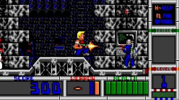
 For the last two and a half years, [Nikolai Wuttke] has been doing exactly that for 1993’s Duke Nukem II. The end result is RigelEngine, an open source drop-in replacement for the original game binary that not only runs on a modern Windows, Linux, or Mac OS machine, but manages to improve on the original in a number of ways. An accomplishment made even more impressive once you learn that the original source code for the game has been lost to time, and that he had to do everything blind.
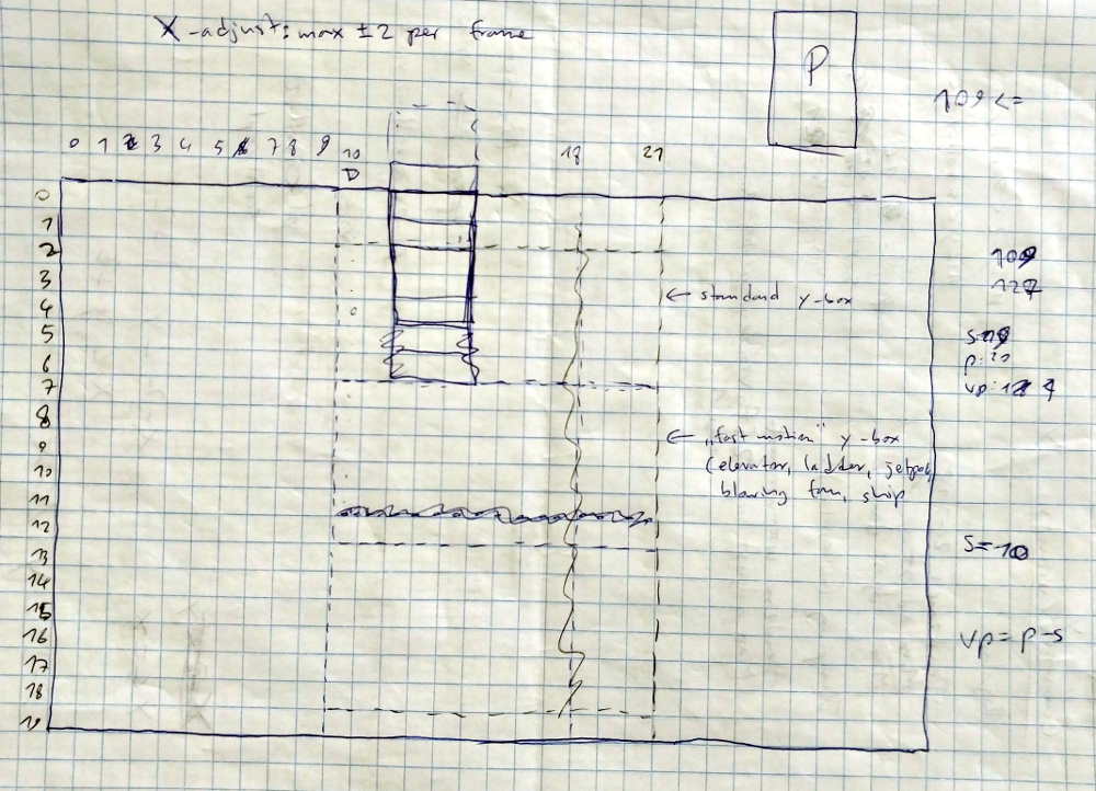
In a blog post chronicling his progress so far, [Nikolai] explains the arduous process he used to make sure his re-implementation was as accurate as possible to the original game. He spent untold hours studying the original game’s disassembled code in Ida Pro, handwriting out pages of notes and pseudocode as he tried to understand what was happening behind the scenes. Once a particular enemy or element of the game was implemented in RigelEngine, he’d record the gameplay from his version and compare it to the original frame by frame so he could fine tune the experience.
So what’s the end result of more than two years of work and over 25K lines of code? Thanks to the incredible advancements in computing power since the game’s release nearly 30 years ago, [Nikolai] has managed to remove the need for loading screens. His engine is also capable of displaying an unlimited number of particle effects on the screen at once, and multiple sound effects can now be played simultaneously. In the future he’s looking to implement smooth character movement (in the original game, movement was in 8 pixel increments) and adaptive volume for sound effects based on their distance from Duke. Ultimately, RigelEngine should be able to replace the original graphics with new high resolution textures once some issues with the rendering buffer gets sorted out.
It’s hard to overstate how important some of these classic games are to those who grew up playing them. With John Romero still releasing DLC for the original DOOM and hackers disassembling nearly 40 year old games to fix bugs, it doesn’t seem like they’re in any danger of being forgotten.
Continue reading “Hail To The King, Baby: Reverse Engineering Duke”