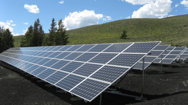
Scanning electron micrograph of a microfabricated lens array

Getting A Fly’s-Eye View With Microfabricated Lens Arrays

Atomic force microscopy, laser ablation, and etching with a witches brew of toxic chemicals: sounds like [Zachary Tong] has been playing in the lab again, and this time he found a way to fabricate arrays of microscopic lenses as a result.

Like many of the best projects, [Zach]’s journey into micro-fabrication started with a happy accident. It happened while he was working on metal-activated chemical etching (MACE), which uses a noble metal catalyst to selectively carve high-aspect-ratio features in silicon. After blasting at a silver-coated silicon wafer with a laser, he noticed the ablation pits were very smooth and uniform after etching. This led him to several hypotheses about what was going on, all of which he was able to test.

The experiments themselves are pretty interesting, but what’s really cool is that [Zach] realized the smooth hemispherical pits in the silicon could act as a mold for an array of microscopic convex lenses. He was able to deposit a small amount of clear silicone resin into the mold by spin-coating, and (eventually) transfer the microlens array to a glass slide. The lenses are impressively small — hundreds of them over only a couple hundred square microns — and pretty well-formed. There’s always room for improvement, of course, but for an initial attempt based on a serendipitous finding, we’d call it a win. As for what good these lenses are, your guess is as good as ours. But novel processes like these tend to find a way to be useful, and the fact that this is coming out of a home lab doesn’t change that fact.

We find this kind of micro-fabrication fascinating. Whether it’s making OLED displays, micro-machining glass with plasma, or even rolling your own semiconductors, we can’t get enough of this stuff.

Continue reading “Getting A Fly’s-Eye View With Microfabricated Lens Arrays”

Garage Semiconductor Fab Gets Reactive-Ion Etching Upgrade

It’s a problem that few of us will likely ever face: once you’ve built your first homemade integrated circuit, what do you do next? If you’re [Sam Zeloof], the answer is clear: build better integrated circuits.

At least that’s [Sam]’s plan, which his new reactive-ion etching setup aims to make possible. While his Z1 dual differential amplifier chip was a huge success, the photolithography process he used to create the chip had its limitations. The chemical etching process he used is a bit fussy, and prone to undercutting of the mask if the etchant seeps underneath it. As its name implies, RIE uses a plasma of highly reactive ions to do the etching instead, resulting in finer details and opening the door to using more advanced materials.

[Sam]’s RIE rig looks like a plumber’s stainless steel nightmare, in the middle of which sits a vacuum chamber for the wafer to be etched. After evacuating the air, a small amount of fluorinated gas — either carbon tetrafluoride or the always entertaining sulfur hexafluoride — is added to the chamber. A high-voltage feedthrough provides the RF energy needed to create a plasma, which knocks fluorine ions out of the process gas. The negatively charged and extremely reactive fluorine ions are attracted to the wafer, where they attack and etch away the surfaces that aren’t protected by a photoresist layer.

It all sounds simple enough, but the video below reveals the complexity. There are a lot of details, like correctly measuring vacuum, avoiding electrocution, keeping the vacuum pump oil from exploding, and dealing with toxic waste products. Hats off to [Sam’s dad] for pitching in to safely pipe the exhaust gases through the garage door. This ties with [Huygens Optics]’s latest endeavor for the “coolest things to do with fluorine” award.

Continue reading “Garage Semiconductor Fab Gets Reactive-Ion Etching Upgrade”

Decapping Components Hack Chat With John McMaster

Join us on Wednesday, March 10 at noon Pacific for the Decapping Components Hack Chat with John McMaster!

We treat them like black boxes, which they oftentimes are, but what lies beneath the inscrutable packages of electronic components is another world that begs exploration. But the sensitive and fragile silicon guts of these devices can be hard to get to, requiring destructive methods that, in the hands of a novice, more often than not lead to the demise of the good stuff inside.

To help us sort through the process of getting inside components, John McMaster will stop by the Hack Chat. You’ll probably recognize John’s work from Twitter and YouTube, or perhaps from his SiliconPr0n.org website, home to beauty shots of some of the chips he has decapped. John is also big in the reverse engineering community, organizing the Mountain View Reverse Engineering meetup, a group that meets regularly to discuss the secret world of components. Join us as we talk to John about some of the methods and materials used to get a look inside this world.

join-hack-chatOur Hack Chats are live community events in the Hackaday.io Hack Chat group messaging. This week we’ll be sitting down on Wednesday, March 10 at 12:00 PM Pacific time. If time zones have you tied up, we have a handy time zone converter.

Click that speech bubble to the right, and you’ll be taken directly to the Hack Chat group on Hackaday.io. You don’t have to wait until Wednesday; join whenever you want and you can see what the community is talking about.
Continue reading “Decapping Components Hack Chat With John McMaster”

The Dark Side Of Solar Power

Everybody loves solar power, right? It’s nice, clean, renewable energy that’s available pretty much everywhere the sun shines. If only the panels weren’t so expensive. Even better, solar is now the cheapest form of electricity for companies to build, according to the International Energy Agency. But solar isn’t all apples and sunshine — there’s a dark side you might not know about. Manufacturing solar panels is a dirty process from start to finish. Mining quartz for silicon causes the lung disease silicosis, and the production of solar cells uses a lot of energy, water, and toxic chemicals.

The other issue is that solar cells have a guanteed life expectancy of about 25 years, with average efficiency losses of 0.5% per year. If replacement begins after 25 years, time is running out for all the panels that were installed during the early 2000s boom. The International Renewable Energy Agency (IREA) projects that by 2050, we’ll be looking at 78 million metric tons of bulky e-waste. The IREA also believe that we’ll be generating six million metric tons of new solar e-waste every year by then, too. Unfortunately, there are hardly any measures in place to recycle solar panels, at least in the US.

How are solar panels made, anyway? And why is it so hard to recycle them? Let’s shed some light on the subject.

Continue reading “The Dark Side Of Solar Power”

Reverse Engineering The Charge Pump Of An 8086 Microprocessor

You’d think that the 8086 microprocessor, a 40-year-old chip with a mere 29,000 transistors on board that kicked off the 16-bit PC revolution, would have no more tales left to tell. But as [Ken Shirriff] discovered, reverse engineering the chip from die photos reveals some hidden depths.

The focus of [Ken]’s exploration of the venerable chip is the charge pump, a circuit that he explains was used to provide a bias voltage across the substrate of the chip. Early chips generally took this -5 volt bias voltage from a pin, which meant designers had to provide a bipolar power supply. To reduce the engineering effort needed to incorporate the 8086 into designs, Intel opted for an on-board charge pump to generate the bias voltage. The circuit consists of a ring oscillator made from a trio of inverters, a pair of transistors, and some diodes to act as check valves. By alternately charging a capacitor and switching its polarity relative to the substrate, the needed -5 volt bias is created.

Given the circuit required, it was pretty easy for [Ken] to locate it on the die. The charge pump takes up a relatively huge amount of die space, which speaks to the engineering decisions Intel made when deciding to include it. [Ken] drills down to a very low level on the circuit, with fascinating details on how the MOSFETs were constructed, and why eight transistors were used instead of two diodes. As usual, his die photos are top quality, as are his explanations of what’s going on down inside the silicon.

If you’re somehow just stumbling upon [Ken]’s body of work, you’re in for a real treat. To get you started, you’ll want to check out how he found pi baked into the silicon of the 8087 coprocessor, or perhaps his die-level exploration of different Game Boy audio chips.

Jan Czochralski And The Silicon Revolution

If you were to travel back in time to the turn of the previous century and try to convince the average person that the grains of sand on just about any beach would be the basis of an industry worth hundreds of billions of dollars within 100 years, they’d probably have thought you were crazy. Aside from being coarse, rough, and irritating, sand is everywhere, and convincing anyone of its value would be a hard sell, unless your interlocutor was a real estate visionary with an appreciation of the future value of seaside property and a lot of patience.

Fast forward to our time, and we all know the value of the material that comes from common quartz sand: silicon, specifically the ultra-purified crystals of silicon that end up as the wafers we depend on to build the circuitry of life. The trip from beach to chip foundry is a long and non-obvious one which would not have been possible without the insights of an undistinguished Polish student and one-time druggist who discovered the process that made the Information Age possible: Jan Czochralski.

Continue reading “Jan Czochralski And The Silicon Revolution”

Chip Decapping The Easy Way

Chip decapping videos are a staple of the hacking world, and few things compare to the beauty of a silicon die stripped of its protective epoxy and photographed through a good microscope. But the process of actually opening that black resin treasure chest seems elusive, requiring as it does a witch’s brew of solvents and acids.

Or does it? As [Curious Marc] documents in the video below, a little heat and some finesse are all it takes, at least for some chips. The method is demonstrated by [Antoine Bercovici], a paleobotanist who sidelines as a collector of old chips. After removing chips from a PCB — he harvested these chips from an old PlayStation — he uses hot air to soften the epoxy, and then flexes the chip with a couple of pairs of pliers. It’s a bit brutal, but in most of the Sony chips he tried for the video, the epoxy broke cleanly over the die and formed a cleavage plane that allowed the die to be slipped out cleanly. The process is not unlike revealing fossils in sedimentary rocks, a process that he’s familiar with from his day job.

He does warn that certain manufacturers, like Motorola and National, use resins that tend to stick to the die more. It’s also clear that a hairdryer doesn’t deliver enough heat; when they switched to a hot air rework station, the success rate went way up.

The simplicity of this method should open the decapping hobby up to more people. Whether you just want to take pretty pictures or if reverse engineering is on your mind, put the white fuming nitric acid down and grab the heat gun instead.

Continue reading “Chip Decapping The Easy Way”