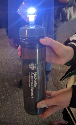
The Hackaday Superconference was last weekend, and it was the greatest hardware con on the planet. What can you build out of a conference badge? If you answered “a resin-based 3D printer” you would have won a prize. If you decided to put your badge in a conference water bottle and make a stun gun you’d receive adoration of all in attendance. Yeah, it got that crazy.
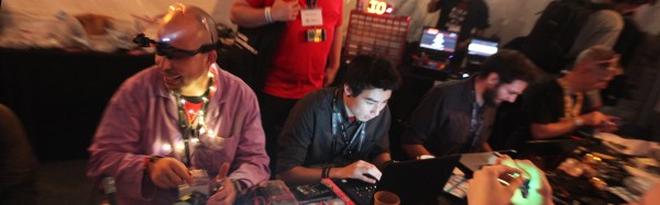
At other tech conferences, you’ll find gaggles of nerds sitting around a table with MacBooks and Thinkpads. The Superconference is different. Here, you’ll find soldering irons, tackle boxes filled with components, and loose WS2812s scattered about the floor. The smell of solder flux wafts through the air. You detect a hint of ozone.
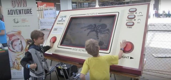
The depth and breadth of hacks that came out of this were simply stunning. We a binocular virtual reality hack, an internet trolling badge, blinky add-on boards, audio add-on boards, a film festival was shot on the badge, and much more which you’ll find below.
We have started a Badge Hacks list and want to see details of all of the hacks. So if you were at Supercon be sure to publish them on Hackaday.io and send a DM to be added to the list.
Starting Up An Extra Day of Hacking
To get all of this creativity rolling we did something a bit different for this year’s Superconference. Instead of opening the doors up on Saturday morning, we set up a badge hacking area and party on Friday afternoon. The drinks flowed like the meniscus on a properly soldered lead, and by 2pm on Friday, everyone was hacking firmware on the incredible camera badge for this year’s con.


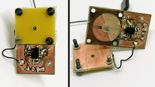
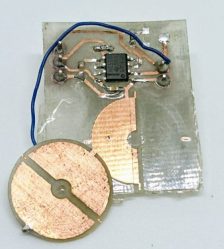
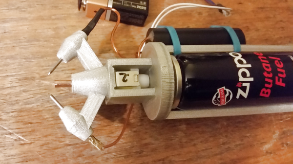
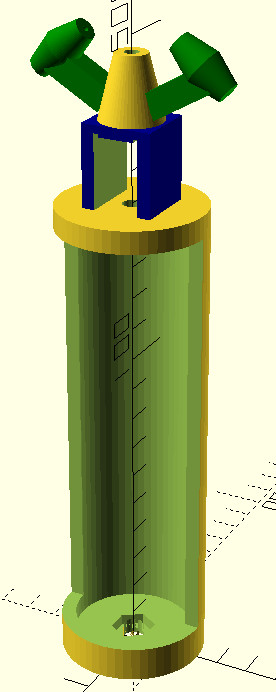
We didn’t stop on Friday. The Superconference is a hardware hacking conference, and that meant we brought out the soldering irons, experimented with melting aluminum with gallium, reflowed a few boards, and created a few deadbug LED cubes. This went on all weekend.
Continue reading “What Actually Happens At A Hardware Hacking Con”