Last week, the US Department of Transportation and FAA released their rules governing drones, model aircraft, unmanned aerial systems, and quadcopters – a rose by any other name will be regulated as such. Now that the online registration system is up and running.
The requirements for registering yourself under the FAA’s UAS registration system are simple: if you fly a model aircraft, drone, control line model, or unmanned aerial system weighing more than 250g (0.55 lb), you are compelled under threat of civil and criminal penalties to register.
This is, by far, one of the simplest rules ever promulgated by the FAA, and looking at the full text shows how complicated this rule could have been. Representatives from the Academy of Model Aircraft, the Air Line Pilots Association, the Consumer Electronics Association weighed in on what types of aircraft should be registered, how they should be registered, and even how registration should be displayed.
Considerable attention was given to the weight limit; bird strikes are an issue in aviation, and unlike drones, bird strikes have actually brought down airliners. The FAA’s own wildlife strike report says, “species with body masses < 1 kilogram (2.2 lbs) are excluded from database,”. The Academy of Model Aircraft pushed to have the minimum weight requiring registration at two pounds, citing their Park Flyer program to define what a ‘toy’ is.
Rules considering the payload carrying ability of an unmanned aerial system were considered, the inherent difference between fixed wing and rotors or quadcopters was considered, and even the ability to drop toy bombs was used in the decision-making process that would eventually put all remotely piloted craft weighing over 250g under the FAA’s jurisdiction. We must at least give the FAA credit for doing what they said they would do: regulate drones in a way that anyone standing in line at a toy store could understand. While the FAA may have crafted one of the simplest rules in the history of the administration, this rule might not actually be legal.
Continue reading “Here’s The Reason The FAA’s Drone Registration System Doesn’t Make Sense” →


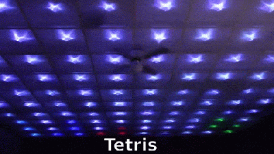 Disco Floor’s are passé. [dennis1a4] turned them upside down and built an awesome
  The hard part was wiring up all of the 160 LED pixels. Instead of mounting the 5050 SMD LED’s on PCBs, [dennis1a4] wired them all up “dead bug” style. Each pixel has one LED, a 100nF decoupling capacitor, and 91 ohm resistors in series with the Data In and Data Out pins – these apparently help prevent ‘ringing’ on the data bus. Check the video for his radical soldering method. Each SMD LED was clamped in a machine shop vice, and the other three parts with their leads preformed were soldered directly to the LED pins.