Living The Dream: New PCB For A Dirt-Cheap Calculator Watch

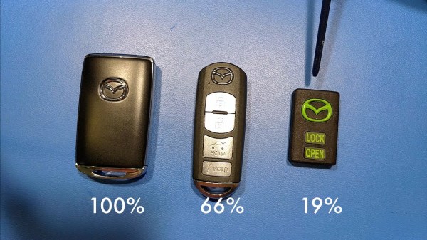
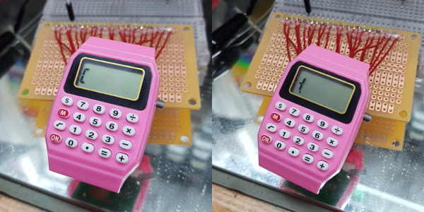
Well, this hack has us tickled pink. We love the idea of buying some really cheap piece of technology and doing something amazing with it, and this is a textbook example of that. [davedarko] found the cutest little calculator watch on Ali Express and is working on making a new PCB for it. The plan is to use an ARM processor and Arduino and add a few extras like 24-hour mode and a pink (or potentially RGB) backlight. The new brain will be an ATSAML22G18A, which has an on-board LCD controller and exactly one I/O pin to spare without charlieplexing the buttons.

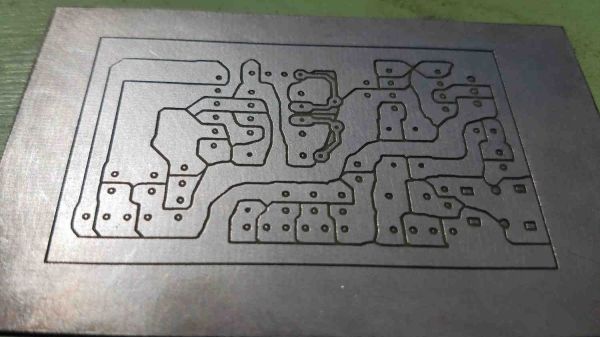
One of [davedarko]’s primary goals is to keep the LCD and figure out how to talk to it. The first order of business was reverse engineering the watch’s LCD controller by sussing out the secrets from beneath the black blob of epoxy. This was an eye-opening experience as [davedarko] had never worked directly with LCDs before. A strange reading made him bust out the oscilloscope. Long-ish and informative story short, [davedarko] found out that it uses a bias of 1/2 for generating the wave necessary to multiplex the segments and keep the signal alternating. This is definitely one to watch!

We love timepieces around here and have seen all kinds of hacks, especially on Casio watches. Want dark mode? Done. Enable the hidden countdown timer? We’ve got that, too. And have you ever wondered just how water-resistant the F91W is?

Build A Barebones 68000

The 68000 chip was ubiquitous in the computing world well past its heyday in the 1980s. It was used as the basis for many PCs and video game consoles, and even in embedded microcontrollers. Now, one of its niche applications is learning about the internal functions of computers. 68000 builds are fairly common when building homebrew computers from scratch, but projects like these can be complicated and quickly get out of hand. This 68000 project, on the other hand, gets the job done with the absolute minimum of parts and really dives into the assembly language programming on these chips. (Google Translate from Spanish)

[osbox68] built this computer by first simulating its operation. Once he was satisfied with that, the next step was to actually build the device. Along with the MC68008 it only uses two other TTL chips, a respectable 32 kilobytes of ram, and additionally supports a serial port and an expansion bus. A few 74-series chips round out the build including a 74HC574 used for debugging support. With a custom PCB to tie everything together, it’s one of the most minimal 68000 builds we’ve seen that still includes everything needed to be completely functional.

After all, including the TTL and 74XX chips the entire circuit board only uses 10 integrated circuits and a few other passive elements for a completely functional retro computer. [osbox68] also includes complete schematics for building a PCB based on these chips to make construction that much easier. Of course, emulating an old microcontroller instead of using TTL components can save a lot of real estate on a PCB especially if you’re using something like an FPGA.

From Printer To Vinyl Cutter

Some might look at a cheap inkjet printer and see a clunky device that costs more to replace the ink than to buy a new one. [Abhishek Verma] saw an old inkjet printer and instead saw a smooth gantry and feed mechanism, the perfect platform to build his own DIY vinyl cutter.

The printer was carefully disassembled. The feed mechanism was reworked to be driven by a stepper motor with some 3D printed adapter plates. A solenoid-based push/pull mechanism for the cutting blade was added with a 3D printed housing along with a relay module. An Arduino Uno takes in commands from a computer with the help of a CNC GRBL shield.

What we love about this build is the ingenuity and reuse of parts inside the old printer. For example, the old PCB was cut and connectors were re-used. From the outside, it’s hard to believe that HP didn’t manufacture this as a vinyl cutter.

If you don’t have a printer on hand, you can always use your CNC as a vinyl cutter. But if you don’t have a CNC, [Abhishek] shares all the STL files for his cutter as well as the schematic. Video after the break.

Continue reading “From Printer To Vinyl Cutter”

Using Heaters To Display Time

We’re always fans of interesting clock builds around here, whether it’s a word clock, marble clock, or in this case a clock using a unique display method. Of course, since this is a build by Hackaday’s own [Moritz v. Sivers] the display that was chosen for this build was a custom thermochromic display. These displays use heat-sensitive material to change color, and his latest build leverages that into one of the more colorful clock builds we’ve seen.

The clock’s display is built around a piece of thermochromic film encased in clear acrylic. The way the film operates is based on an LCD display, but using heat to display the segments. For this build, as opposed to his previous builds using larger displays, he needed to refine the method he used for generating the heat required for the color change. For that he swapped out the Peltier devices for surface mount resistors and completely redesigned the drivers and the PCBs around this new method.

Of course, the actual clock mechanism is worth a mention as well. The device uses an ESP8266 board to handle the operation of the clock, and it is able to use its wireless capabilities to get the current time via NTP. All of the files needed to recreate this are available on the project page as well, including code, CAD files, and PCB layouts. It’s always good to have an interesting clock around your home, but if you’re not a fan of electronic clocks like this we can recommend any number of mechanical clocks as well.

Continue reading “Using Heaters To Display Time”

Open-Source Method Makes Possible Two-Layer PCBs With Through-Plating At Home

If the last year and its supply chain problems have taught us anything, it’s the value of having a Plan B, even for something as commoditized as PCB manufacturing has become. If you’re not able to get a PCB made commercially, you might have to make one yourself, and being able to DIY a dual-layer board with plated-through vias might just be a survival skill worth learning.

Granted, [Hydrogen Time]’s open-source method, which he calls “Process 01”, is something that he has been working on for years now. And it’s quite the feat of chemistry, which may require you to climb a steep learning curve, depending on how neglected the skills from high school or college chemistry are. But for as complex as Process 01 is, it’s actually pretty straightforward, and the first video below covers it in extreme detail. It starts with a drilled double-sided copper-clad board, which after cleaning is given a bath in palladium chloride. A follow-up dunk in stannous chloride leaves a thin film of palladium metal over all surfaces, even the via walls. This then acts as a catalyst for electroless copper plating in a solution of copper sulfate, followed by an actual electroplating step to thicken the copper plating.

After more washing, photoresist is applied to define the traces as well as to protect the now-plated vias, the board is etched, and a solder mask layer is applied. The boards might not be mistaken for commercial PCBs, but they’re pretty darn good, and as [Hydrogen Time] states, Process 01 is only a beginning. We expect this will be improved and streamlined as time goes by.

Fair warning, though — some steps require a fume hood to be performed safely. Luckily, we’ve got that covered. Sort of.

Continue reading “Open-Source Method Makes Possible Two-Layer PCBs With Through-Plating At Home”

Custom Keyfob Fixes Mazda Design Mistake

While Mazda has made some incredible advances in fuel efficient gasoline engines over the past few years, their design group seems to have fallen asleep at the wheel in the meantime, specifically in regards to the modern keyfob design. The enormous size and buttons on the side rather than the face are contrary to what most people need in a keyfob: small size and buttons that don’t accidentally get pressed. Luckily, though, the PCB can be modified with some effort.

This particular keyfob has a relatively simple two-layer design which makes it easy to see where the connections are made. [Hack ‘n’ Tink] did not need the panic button or status LED which allowed him to simply cut away a section of the PCB, but changing the button layout was a little trickier. For that, buttons were soldered to existing leads on the face of the board using 30-gage magnet wire and silicone RTV. From there he simply needed to place the battery in its new location and 3D print the new enclosure.

The end result is a much smaller form factor keyfob with face buttons that are less likely to accidentally get pressed in a pocket. He also made sure that the battery and button relocation wouldn’t impact the antenna performance. It’s a much-needed improvement to a small but crucial part of the car; the only surprise is that a company that’s usually on point with technology and design would flop so badly on such a critical component.

Thanks to [Brian] for the tip!

Continue reading “Custom Keyfob Fixes Mazda Design Mistake”

JavaScript App Uses Advanced Math To Make PCBs Easier To Etch

We all remember the litany from various math classes we’ve taken, where frustration at a failure to understand a difficult concept bubbles over into the classic, “When am I ever going to need to know this in real life?” But as we all know, even the most esoteric mathematical concepts have applications in the real world, and failure to master them can come back to haunt you.

Take Voronoi diagrams, for example. While we don’t recall being exposed to these in any math class, it turns out that they can be quite useful in a seemingly unrelated area: converting PCB designs into easy-to-etch tessellated patterns. Voronoi diagrams are in effect a plane divided into different regions, or “cells”, each centered on a “seed” object. Each cell is the set of points that are closer to a particular seed than they are to any other seed. For PCBs the seeds can be represented by the traces; dividing the plane up into cells around those traces results in a tessellated pattern that’s easily etched.

To make this useful to PCB creators, [Craig Iannello] came up with a JavaScript application that takes an image of a PCB, tessellates the traces, and spits out G-code suitable for a laser engraver. A blank PCB covered with a layer of spray paint, the tessellated pattern is engraved into the paint, and the board is etched and drilled in the usual fashion. [Craig]’s program makes allowances for adding specific features to the board, like odd-shaped pads or traces that need specific routing.

This isn’t the first time we’ve seen Voronoi diagrams employed for PCB design, but the method looks so easy that we’d love to give it a try. It even looks as though it might work for CNC milling of boards too.