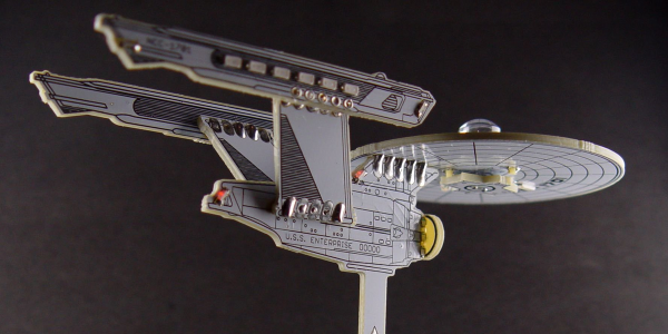
This Home-Etched ARM Dev Board Is A Work Of Art

One of the step changes in electronic construction at our level over the last ten or fifteen years has been the availability of cheap high-quality printed circuit boards. What used to cost hundreds of dollars is now essentially an impulse buy, allowing the most intricate of devices to be easily worked with. Many of us have put away our etching baths for good, often with a sigh of relief.

We’re pleased that [Riyas] hasn’t though, because they’ve etched an STM32 dev board that if we didn’t know otherwise we’d swear had been produced professionally. It sports a 176-pin variant of an STM32F4 on a single-sided board, seemingly without the annoying extra copper or lack-of-copper that we remember from home etching. We applaud the etching skill that went into it, and we’ll ignore the one or two boards that didn’t go entirely to plan. A coat of green solder mask and some tinning, and it looks for all the world as though it might have emerged from a commercial plant. All the board files are available to download along with firmware samples should you wish to try making one yourself, though we won’t blame you for ordering it from a board house instead.

It’s always nice to see that single board computers are not the sole preserve of manufacturers. If the RC2014 Micro doesn’t isn’t quite your style, there’s always the Blueberry Pi which features a considerably higher penguin quotient.

The Benefits And Pitfalls Of Using PCBs As An Enclosure

[Mastro Gippo] found himself in a pickle recently, with the development of an enclosure for the Prism electric vehicle charger. The body had been sorted out, but the front cover needed work. It had to be visually appealing, and ideally should provide the user feedback on the charging process. After some thought, [Mastro] decided to explore the possibilities of using a PCB as a part of a commerical product enclosure.

For a variety of reasons, using a specially designed PCB was an attractive solution for the team’s enclosure. Wanting something cost effective, easily customizable, and something that would help with emissions compliance, a PCB seemed like a great idea. With this in mind, [Mastro] prepared a series of prototypes. These feature see-through sections for LEDs to shine through, as well as a capacitive button and gold-plated logo. The fact that the front cover is a PCB makes the integration of the electronic components a cinch.

Before heading into full production, [Mastro] began to question why this technique isn’t used more often. Deciding to research further, [Bunnie Huang] was tapped to provide some advice on the concept. Noting that there can be issues with lead content, as well as the fact that PCBs aren’t often produced with proper regard to aesthetics, there were some pitfalls to the idea. Additionally, ESD testing can be difficult, while the in-built capacitive button would face issues in wet conditions.

None of these are showstoppers however, and [Mastro] has persevered, combining the front cover PCB with an adhesive plastic sheet for added protection. We fully expect that if more manufacturers explore this route, it may be a more viable technique in future. It’s also a great example of knowing when to ask others for help – it’s not the first time we’ve learned from [Bunnie’s] broad experience!

These Tips Make Assembling A Few Hundred PCBs Easier

There are a few common lessons that get repeated by anyone who takes on the task of assembling a few hundred PCBs, but there are also unique insights to be had. [DominoTree] shared his takeaways after making a couple hundred electronic badges for DEFCON 26 (that’s the one before the one that just wrapped up, if anyone’s keeping track.) [DominoTree] assembled over 200 Telephreak badges and by the end of it he had quite a list of improvements he wished he had made during the design phase.

Some tips are clearly sensible, such as adding proper debug and programming interfaces, or baking an efficient test cycle into the firmware. Others are not quite so obvious, for example “add a few holes to your board.” Holes can be useful in unexpected ways and cost essentially zero. Even if the board isn’t going to be mounted to anything, a few holes can provide a way to attach jigs or other hardware like test fixtures.

[DominoTree] ended up having to attach multiple jumper wires to reprogram boards after assembly, and assures us that “doing this a bunch of times really sucked.”
Other advice is more generic but no less important, as with “eliminate as many steps as possible.” Almost anything adds up to a significant chunk of time when repeated hundreds of times. To the basement hacker, something such as pre-cut and pre-tinned wires might seem like a shameful indulgence. But cutting, stripping, tinning, then hand-soldering a wire adds up to significant time and effort by iteration number four hundred (that’s two power wires per badge) even if one isn’t staring down a looming deadline.

[DominoTree] also followed up with additional advice on making assembly easier. Our own [Brian Benchoff] has also shared his observations on the experience of developing and assembling a large number of Hackaday Superconference badges, including what it took to keep things moving along when inevitable problems surfaced.

You don’t need to be making batches of hundreds for these lessons to pay off, so keep them in mind and practice them on your next project.

You Didn’t See Graphite Around This Geiger Counter

Even if you don’t work in a nuclear power plant, you might still want to use a Geiger counter simply out of curiosity. It turns out that there are a lot of things around which emit ionizing radiation naturally, for example granite, the sun, or bananas. If you’ve ever wondered about any of these objects, or just the space you live in, it turns out that putting together a simple Geiger counter is pretty straightforward as [Alex] shows us.

The core of the Geiger counter is the tube that detects the radiation. That’s not something you’ll be able to make on your own (probably) but once you have it the rest of the build comes together quickly. A few circuit boards to provide the tube with the high voltage it needs, a power source, and a 3D printed case make this Geiger counter look like it was ordered from a Fluke catalog.

The project isn’t quite finished ([Alex] is still waiting on a BNC connector to arrive) but seems to work great and isn’t too complicated to put together, as far as Geiger counters go. He did use a lathe for some parts which not everyone will have on hand, but a quick trip to a makerspace or machinist will get you that part too. We’ve seen some other parts bin Geiger counters too, so there’s always a way around things like this.

Another Way To Make PCBs At Home

One of the more popular ways of rolling out your own custom PCB is to simply create the model in your CAD program of choice and send it off to a board manufacturer who will take care of the dirty work for you. This way there is no need to deal with things like chemicals, copper dust, or maintaining expensive tools. A middle ground between the board manufacturer and a home etching system though might be what [igorfonseca83] has been doing: using an inexpensive laser engraver to make PCBs for him.

A laser engraver is basically a low-power laser CNC machine that’s just slightly too weak to cut most things that would typically go in a laser cutter. It turns out that the 10W system is the perfect amount of energy to remove a mask from a standard PCB blank, though. This in effect takes the place of the printer in the old toner transfer method, and the copper still has to be dissolved in a chemical solution, but the results are a lot more robust than trying to modify a printer for this task.

If you aren’t familiar with the days of yore when homebrew PCBs involved a standard desktop printer, many people still use this method, although the results can be mixed based on printer reliability. If you want to skip the middleman, and the need for a chemical bath, a more powerful laser actually can cut the traces for you, too.

Continue reading “Another Way To Make PCBs At Home”

Control The Suck With This Manual Vacuum Pick-And-Place Tool

The tapes that surface-mount devices come in may be optimized for automated pick and place, but woe betide those who try to dig components out manually. No matter what size package, the well on the tape seems to be just a wee bit too small to allow tweezers to grip it, so you end up picking the thing up edgewise or worse, pinching too tight and launching the tiny thing into The Void. We hope you ordered extra.

Such circumstances are why vacuum handlers were invented, but useful as they are for picking and placing SMDs, they aren’t perfect. [Steve Gardener]’s sub-optimal experience with such tools led him to build this custom vacuum pick-and-place tool. It’s based on an off-the-shelf Weller unit, of which only the handpiece remains. A bigger, more powerful vacuum pump is joined in a custom enclosure by a PCB with a PIC18F13K22 microcontroller, a power supply, a solenoid to control the vacuum, and a relay to switch the pump. A footswitch starts the pump and closes the vacuum vent; letting off the pedal opens the vent to drop the part, while the pump keeps running for a variable time. This lets him rapidly work through a series of parts without having to build vacuum back up between picks. The video below shows the build and the tool in action.

We love the idea of this tool, and the polished look is pretty slick too. If manual pick-and-place isn’t for you, though, maybe converting a 3D-printer into an automated PnP is something to check out.

Continue reading “Control The Suck With This Manual Vacuum Pick-And-Place Tool”

Quick-Turn PCB Fab Hack Chat

Join us on Wednesday, July 31st at noon Pacific for the Quick-Turn PCB Fab Hack Chat with Mihir Shah!

We’ve all become used to designing a PCB and having it magically appear at our doorstep – after a fashion. Modern PCB fabs rely on economies of scale to deliver your design cheaply, at the expense of time – the time it takes to put enough orders onto a panel, and the time it takes to ship the finished boards from Far, Far Away.

Not everyone has that kind of time to burn, though. That’s where quick-turn fabs come in. These manufacturers specialize in getting boards to their customers as quickly as possible, helping them deal with sudden design changes or supporting specialty applications for customers.

It’s a niche industry, but an important one, and Royal Circuits is at the forefront. Mihir Shah is Director of Special Projects there, and he’s deep into the business of getting PCBs to customers as quickly as possible. He’ll drop by the Hack Chat to answer all your questions about how the quick-turn industry fits into the electronics manufacturing ecosystem, and to show off some of the tools of the future that they’re developing and investing in to streamline PCB design and analysis – from DebuggAR to PCBLayout.com, and more.

join-hack-chatOur Hack Chats are live community events in the Hackaday.io Hack Chat group messaging. This week we’ll be sitting down on Wednesday July 31 at 12:00 PM Pacific time. If time zones have got you down, we have a handy time zone converter.

Click that speech bubble to the right, and you’ll be taken directly to the Hack Chat group on Hackaday.io. You don’t have to wait until Wednesday; join whenever you want and you can see what the community is talking about.