Make Your Own MIDI Controller With An Arduino

Engineers create something out of nothing, and no where is this more apparent than in the creation of customized computer hardware. To make a simple MIDI controller, you need knowledge of firmware design and computer architecture, you need knowledge of mechanical design, and you need to know electronic design. And then you need the actual working knowledge and experience to wield a tool, be it a hammer, laser cutter, or an IDE. [Mega Das] brought together all of these skill to build a MIDI controller. Sure, it’s for bleeps and bloops coming out of a speaker, but take a step back and realize just how awesome it is that any one person could imagine, then implement such a device.

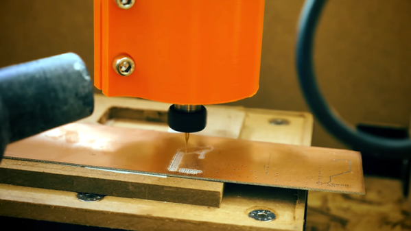
The electronics for this build include a printed circuit board that serves to break out the connections on an Arduino nano to a dozen arcade push buttons, four slide pots, two rotary pots, and a handful of screw terminals to connect everything together. Mechanically, this is a laser-cut box engraved with some fancy graphics and sized perfectly to put everything inside.

Yes, we’ve seen a lot of MIDI controllers built around the Arduino over the years, but this one is in a class by itself. This is taking off-the-shelf parts and customizing them to exactly what you want, and a prodigious example of what is possible with DIY hardware creation. You can check out the build video below.

Continue reading “Make Your Own MIDI Controller With An Arduino”

LEDs Shine Through PCB On This Tiny Word Clock

Everyone seems to love word clocks. Maybe it’s the mystery of a blank surface lighting up to piece together the time in fuzzy format, or maybe it hearkens back to those “find-a-word” puzzles that idled away many an hour. Whatever it is, we see a lot of word clock builds, but there’s something especially about this diminutive PCB word clock that we find irresistible.

Like all fun projects, [sjm4306] found himself going through quite the design process with this one. The basic idea – using a PCB as the mask for the character array – is pretty clever. We’ve always found the laser-cut masks to be wanting, particularly in the characters with so-called counters, those enclosed spaces such as those in a capital A or Q that would be removed by a laser cutter. The character mask PCB [sjm4306] designed uses both the copper and a black solder mask to form the letters, which when lit by the array of SMD LEDs behind it glow a pleasing blue-green color against a dark background. Try as he might, though, the light from adjacent cells bled through, so he printed a stand that incorporates baffles for each LED. The clock looks great and even has some value-added modes, such as a falling characters display a la The Matrix, a Pong-like mode, and something that looks a bit like Tetris. Check out the video below for more details.

We’ve seen word clocks run afoul of the counter problem before, some that solved it by resorting to a stencil font, others that didn’t. We’re impressed by this solution, though, enough so that we hope [sjm4306] makes the PCB files available so we can build one.

Continue reading “LEDs Shine Through PCB On This Tiny Word Clock”

Stuck Designing Two-Layer PCBs? Give Four Layers A Try!

Many readers are certainly familiar with the process for home-etching of PCBs: it’s considered very straightforward, if a little involved, today. This was not the case in my youth, when I first acquired an interest in electronics. At that time, etching even single-sided boards was for “advanced” hobbyists. By the time I started etching my own PCBs, the advanced hobbyists were on to double-sided home-etched boards — the only type not pictured above, because I couldn’t find the one successful example I ever created. I later saw the rise of “bare bones” fabricated PCBs: professionally made fixed size boards with plated-through holes, but no soldermask or silkscreen. Eventually, this gave way to the aggregating PCB services we have now with full two-layer boards, complete with soldermask and silkscreen.

Today, the “advanced” hobbyist may be using four-layer boards, although the four-layer adoption rate is still relatively low – OSH Park produces around 90% two-layer and 10% four-layer, for instance. I think this will inevitably increase, as has been the case with all the previous technologies: the advanced eventually becomes the mainstream. Each of the previous shifts has brought easier design and construction as well as improved performance, and the same will be true as four layers becomes more commonplace.

So, let’s take a look at designing four-layer PCBs. If you’ve never considered one for any of your designs, you may be pleasantly surprised at what little extra cost is involved for all the benefits you gain. Continue reading “Stuck Designing Two-Layer PCBs? Give Four Layers A Try!”

Imitating Art In Life With A Reverse-Engineered Tattoo

In general, tattoo artists are not electrical engineers. That’s fine; the world needs both professions. But when you need a circuit designed, you’re better off turning to an EE rather than a tattoo artist. And you certainly don’t want an EE doing your new ink. Disaster lies that way.

Surprisingly, [Missa]’s tattoo of a heart-shaped circuit turned out at least to be plausible design, even if it’s not clear what it’s supposed to do. So her friend [Jeremy Elson] took up the challenge to create a circuit that looked like the tattoo while actually doing something useful. He had to work around the results of tattoo artistic license, like sending traces off to the board’s edge and stranding surface-mount components without any traces. The artist had rendered an 8-pin DIP device, albeit somewhat proportionally challenged, so [Jeremy] went with an ATtiny85, threw on a couple of SMD resistors and a cap, and placed two LEDs for the necessary blinkenlights. Most of the SMDs are fed from traces on the back of the board that resurface through vias, and a small coin cell hidden on the back powers it. One LED blinks “Happy Birthday [Missa]” in Morse, while the other blinks prime numbers from 2 to 23 – we’ll assume this means it was [Missa]’s 23rd birthday.

There’s a surprising amount of crossover between the worlds of electronics and tattooing. We’ve featured functional temporary tattoo circuits, prison-expedient tattoo guns, and even a CNC tattoo machine.

Continue reading “Imitating Art In Life With A Reverse-Engineered Tattoo”

Create Green, Soldermasked PCBs With Fritzing

Even though you can easily order a PCB from any one of a dozen board houses and have it on your desk in a few weeks, there’s still a need for home-made circuit boards. If it’s because you have very special or strange requirements, you want to save money, or you need to suffer for your art, you can make printed circuit boards at home. You can even apply soldermask. It’s easy, and [Renzo] is here to show you how.

The beginnings of this tutorial cover well-tread territory such as building a CNC router, laying out a circuit, and cutting a piece of single-sided, copper clad board. If you stopped right there, after milling traces into a board, you would have a functioning circuit. But it wouldn’t look good; a piece of copper does not a PCB make, and you need soldermask. That’s where the real work comes in.

Applying the soldermask meant there needed to be places without soldermask, mostly the vias and through-holes. For this, [Renzo] pulled the copper pad layer out of Fritzing, printed it on a transparency sheet, and finally applied the UV-curing soldermask. This came as a kit, and right now, you can get 10 ml of green, red, blue, yellow, and black UV-curing soldermask, and a UV flashlight for ten dollars on the usual Internet shops. This soldermask was lathered on, rolled out, and exposed with the UV flashlight. After a quick wash in acetone, the result is a perfect PCB.

CNC Your Own PCB With This Tutorial

It is getting so easy to order a finished printed circuit board that it is tough to justify building your own. But sometimes you really need a board right now. Or maybe you need a lot of fast iterations so you can’t wait for the postal service. [Thomas Sanladerer] shows how he makes PCBs with a CNC machine and has a lot of good advice in the video below.

He starts with Eagle, although, you could use any creation package. He shows what parameters he changes to make sure the traces don’t get eaten away and how to do the CAM job to get the files required to make the boards. If you don’t use Eagle, you’ll need to infer how to do similar changes and get the same kind of output.

We’ve only heard a few people pronounce Gerber (as in Gerber file) with a soft G sound, but we still knew what he meant. We have the same problem with GIF files. However, once you have Gebers, you can join the video’s workflow about 5 minutes in.

At that point, he uses FlatCAM to convert the Gerbers to a single G-code file that integrates the paths and drill files. There were a few tricks he used to make sure all the tracks are picked up. Other tricks include leveling a spoil board by just milling it down and mounting different size bits. He also has ideas on aligning the Z axis.

Continue reading “CNC Your Own PCB With This Tutorial”

Reverse Engineering Keeps Keck Telescopes On Track

Perched atop a dormant volcano far above the roiling tropical air of the Big Island of Hawai’i sit two of the largest optical telescopes in the world. Each 10-meter main mirror is but a single part of a magnificent machine weighing in at some 400 tons that needs to be positioned with incredible precision. Keeping Keck 1 and Keck 2 in peak operating condition is the job of a team of engineers and scientists, so when the servo amplifiers running the twelve motors that move each scope started to show their age, [Andrew] bit the bullet and rebuilt the obsolete boards from scratch.

The Keck telescopes were built over three decades ago, and many of the parts, including the problematic servo amps, are no longer made. Accumulated wear and tear from constant use and repeated repairs had taken their toll on the boards, from overheated components to lifted solder pads. With only some barely legible schematics of the original amplifiers to go by, [Andrew] reverse engineered new amps. Some substitutions for obsolete components were needed, the PCB design was updated to support SMD parts, and higher-quality components were specified, but the end result is essentially new amplifiers that are plug-in replacements for the original units. This should keep the telescopes on track for decades to come.

Not to sound jealous, but it seems like [Andrew] has a great gig. He’s shared a couple of his Keck adventures before, like the time a failed LED blinded the telescope. He’s also had a few more down-to-earth hacks, like fixing a dodgy LCD monitor and making spooky blinkeneyes for Halloween.