In the world of cheap amateur radio transceivers, the Quansheng UV-K5 can’t be beaten for hackability. But pretty much every hack we’ve seen so far focuses on the firmware. What about the hardware?
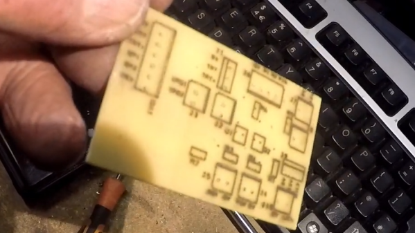
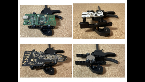
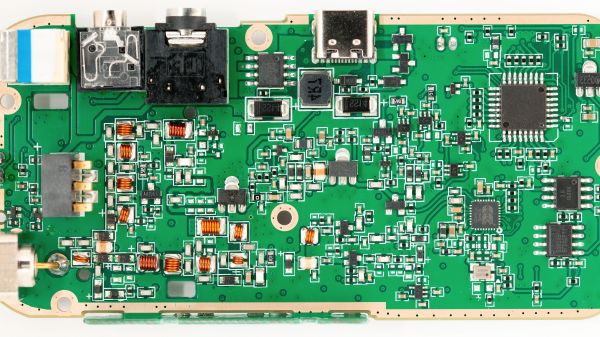
To answer that question, [mentalDetector] enlisted the help of a few compatriots and vivisected a UV-K5 to find out what makes it tick. The result is a complete hardware description of the radio, including schematics, PCB design files, and 3D renders. The radio was a malfunctioning unit that was donated by collaborator [Manuel], who desoldered all the components and measured which ones he could to determine specific values. The parts that resisted his investigations got bundled up along with the stripped PCB to [mentalDetector], who used a NanoVNA to characterize them as well as possible. Documentation was up to collaborator [Ludwich], who also made tweaks to the schematic as it developed.
PCB reverse engineering was pretty intense. The front and back of the PCB — rev 1.4, for those playing along at home — were carefully photographed before getting the sandpaper treatment to reveal the inner two layers. The result was a series of high-resolution photos that were aligned to show which traces connected to which components or vias, which led to the finished schematics. There are still a few unknown components, The schematic has a few components crossed out, mostly capacitors by the look of it, representing unpopulated pads on the PCB.
Hats off to the team for the work here, which should make hardware hacks on the radio much easier. We’re looking forward to what’ll come from this effort. If you want to check out some of the firmware exploits that have already been accomplished on this radio, check out the Trojan Pong upgrade, or the possibilities of band expansion. We’ve also seen a mixed hardware-firmware upgrade that really shines.