Original Controller Ports In Custom Case Means Retro Gaming In Style

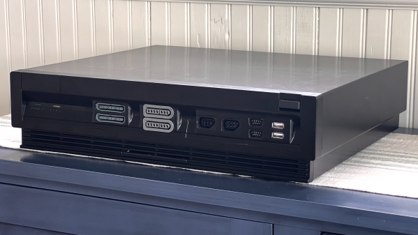
Some careful measuring and a little extra effort can be all that separates what looks like a hack job from a slick end product, and that is apparent in [Eric Sorensen]’s classy retrogaming rig, complete with ports for original console controllers.

Neatly housing these components in a case makes all the difference.

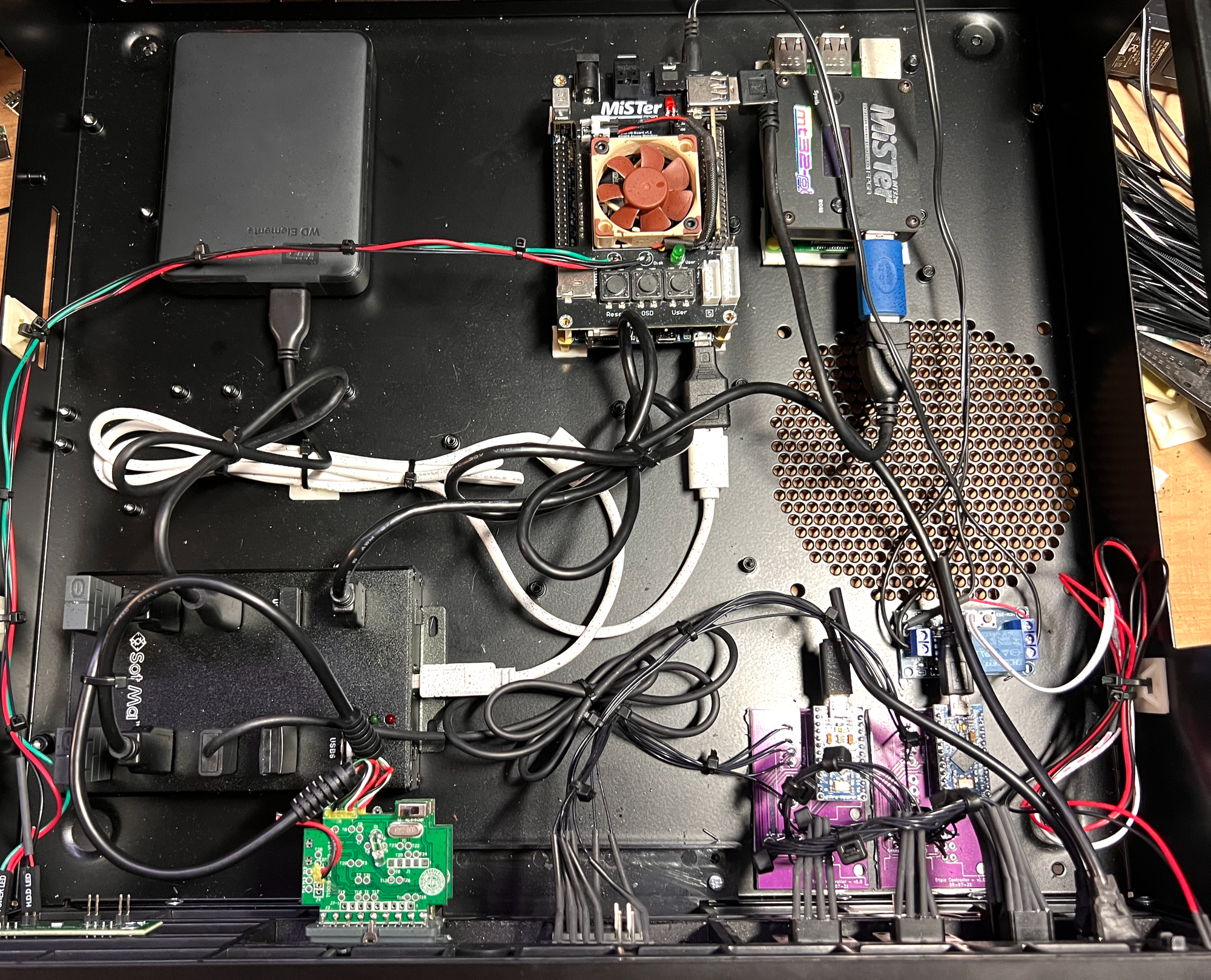
[Eric] likes his vintage gaming, and was terrifically pleased with MiSTer, an open-source project that recreates various classic computers, game consoles and arcade machines using modern FPGA-based hardware. Of course, what makes retro gaming even better is using a platform’s genuine original controllers, which just takes a little extra hardware and wiring.

But [Eric] found that all the required accessories and peripherals started to look awfully cluttered. He solved this issue by packing everything carefully into a specialty PC case called the Checkmate A1500 Plus, which gives off a strong 80s design vibe. As a bonus, the front panels are all removable and that’s where [Eric] decided to house the custom controller ports.

First [Eric] carefully measured each controller connector to create CAD models, then designed matching front panels to house the connectors and 3D printed them. Once that was done, post-processing the panels was a long process of apply Bondo, sand, paint, and repeat as needed. The results looks fantastic, and this project is a prime example of how aesthetics and finish can matter.

Find yourself in a similar situation? [Tom Nardi] has shown us all that 3D prints don’t have to look 3D-printed, and careful application of paint and primer can really put the ‘pro’ in prototyping.

a Pi Pico on a breadboard, running a 7-segment counter gateware, with a 7-segment digit and a pushbutton next to the Pico

Want To Play With FPGAs? Use Your Pico!

Ever want to play with an FPGA, but don’t have the hardware? Now, if you have one of those ever-abundant Pi Picos, you can start playing with Verilog without getting an FPGA board. The FakePGA project by [tvlad1234], based on the Verilator toolkit, provides you with a way to compile Verilog into C++ for the RP2040. FakePGA even integrates RP2040 GPIOs so that they work as digital pins for the simulated GPIOs, making it a significant step up from computer-aided FPGA code simulation

[tvlad1234] provides instructions for setting this up with Linux – Windows, though untested, could theoretically run this through WSL. Maximum clock speed is 5KHz – not much, but way better than not having any hardware to test with. Everything you’d want is in the GitHub repo – setup instructions, Verilog code requirements, and a few configuration caveats to keep in mind.

We cover a lot of projects where FPGAs are used to emulate hardware of various kinds, from ISA cards to an entire Game BoyCPU emulation on FPGAs is basically the norm — it’s just something easy to do with the kind of power that an FPGA provides. Having emulation in the opposite direction is unusual,  though, we’ve seen FPGAs being emulated with FPGAs, so perhaps it was inevitable after all. Of course, if you have neither a Pico nor an FPGA, there’s always browser based emulators.

Continue reading “Want To Play With FPGAs? Use Your Pico!”

A Cycle-Accurate Intel 8088 Core For All Your Retro PC Needs

A problem faced increasingly by retrocomputer enthusiasts everywhere is the supply of chips. Once a piece of silicon goes out of production its demand can be supplied for a time by old stock and second hand parts, but as they become rare so the cost of what can be dubious parts accelerates out of reach. Happily for CPUs at least, there’s a ray of hope in the form of FPGA-based cores which can replace the real thing, and for early PC owners there’s a new one from [Ted Fried]. MCL86 is a cycle accurate Intel 8088 FPGA Core that can be used within an FPGA design or as a standalone in-circuit replacement for a real 8088. It even has a full-speed mode that sacrifices cycle accuracy and can accelerate those 8088 instructions by 400%.

Reading the posts on his blog, it’s clear that this is a capable design, and it’s even been extended with a mode that adds cache RAM to mirror the system memory at the processor’s speed. You can find all the code in a GitHub repository should you be curious enough to investigate for yourself. We’ve pondered in the past where the x86 single board computers are, perhaps it could be projects like this that provide some of them.

A 386 motherboard with a custom ISA card plugged in

Emulate Any ISA Card With A Raspberry Pi And An FPGA

One of the reasons the IBM PC platform became the dominant standard for desktop PCs back in the mid-1980s was its open hardware design, based around what would later be called the ISA bus. Any manufacturer could design plug-in cards or even entire computers that were hardware and software compatible with the IBM PC. Although ISA has been obsolete for most purposes since the late 1990s, some ISA cards such as high-quality sound cards have become so popular among retrocomputing enthusiasts that they now fetch hundreds of dollars on eBay.

So what can you do if your favorite ISA card is not easily available? One option is to head over to [eigenco]’s GitHub page and check out his FrankenPiFPGA project. It contains a design for a simple ISA plug-in card that hooks up to a Cyclone IV FPGA and a Raspberry Pi. The FPGA connects to the ISA bus and implements its bus architecture, while the Pi communicates with the FPGA through its GPIO ports and emulates any card you want in software. [eigenco]’s current repository contains code for several sound cards as well as a hard drive and a serial mouse. The Pi’s multi-core architecture allows it to run several of these tasks at once while still keeping up the reasonably high data rate required by the ISA bus.

In the videos embedded below you can see [eigenco] demonstrating the system on a 386 motherboard that only has a VGA card to hook up a monitor. By emulating a hard drive and sound card on the Pi he is able to run a variety of classic DOS games with full sound effects and music. The sound cards currently supported include AdLib, 8-bit SoundBlaster, Gravis Ultrasound and Roland MT-32, but any card that’s documented well enough could be emulated.

This approach could also come in handy to replace other unobtanium hardware, like rare CD-ROM interfaces. Of course, you could take the concept to its logical extreme and simply implement an entire PC in an FPGA.

Continue reading “Emulate Any ISA Card With A Raspberry Pi And An FPGA”

ICEBlaster: A Drag’n’Drop Bitstream Loader For ICE40

The iCE40 series of FPGAs gets a fair bit of coverage on these pages, largely due to its accessibility (thanks to huge efforts in reverse engineering and open tool chains) and likely also due to Lattice Semiconductors’ attitude to open source in general. Whilst these devices are small and rather limited, you can’t really beat them for a first foray into the subject. They’re plenty beefy enough for many of the simpler FPGA applications. [TinLethax] over on Hackaday.IO has plenty of experience with the devices, and has added another tool to our collective iCE40 arsenal, namely iCEBlaster, a USB mass storage device (MSC) style bootloader for drag-n-drop bitstream loading. The days of needing dedicated special programmers are starting to be numbered, with many chips now presenting a USB mass storage device to the host in order to upload the firmware image.

FPGAs don’t tend to operate this way, needing a device-specific bitstream loading upon start-up, which (unless they have OTP memory) is usually the job of an external configuration memory. iCEBlaster (a play on the Xilinx ByteBlaster programmer, maybe?) runs on the STM32F4xx series devices at least, but should be easily portable to others. The idea is pretty straightforward — dragging a new bitstream file onto the storage device initiates an FPGA target reset, which in turn allows the STM32 to send the bitstream over to the iCE40 via the SPI interface. Nothing more than that.

If you’ve been looking to get into the iCE40, this guide might be a good starting point, and every learning experience needs a good project to drive it, how about running Doom on a softcore RISC-V?

Mis-captured signal transitions shown on the screen of the LA104, with problematic parts circled in red.

When Your Logic Analyzer Can’t Tell Good And Bad Signals Apart

[Avian] has picked up a Miniware LA104 – a small battery-powered logic analyzer with builtin protocol decoders. Such analyzers are handy tools for when you quickly need to see what really is happening with a certain signal, and they’re cheap enough to be sacrificial when it comes to risky repairs. Sadly, he stumbled upon a peculiar problem – the analyzer would show the signal glitching every now and then, even at very low bitrates. Even more surprisingly, the glitches didn’t occur in the signal traces when exported and viewed on a laptop.

A Pulseview window showing that the problem is not present in the exported capturesHe dug into the problem, as [Avian] does. Going through the problem-ridden capture files helped him realize that the glitch would always happen when one of the signal edges would be delayed by a few microseconds relative to other signal edges — a regular occurrence when it comes to digital logic. This seems to stem from compression being used by the FPGA-powered “capture samples and send them” part of the analyzer. This bug only relates to the signal as it’s being displayed on the analyzer’s screen, and turned out that while most of this analyzer’s interface is drawn by the STM32 CPU, the trace drawing part specifically was done by the FPGA using a separate LCD interface.

It would appear Miniware didn’t do enough testing, and it’s impossible to distinguish a good signal from a faulty one when using a LA104 – arguably, the primary function of a logic analyzer. In the best of Miniware traditions, going as far as being hostile to open-source firmware at times, the FPGA bistream source code is proprietary. Thus, this bug is not something we can easily fix ourselves, unless Miniware steps up and releases a gateware update. Until then, if you bought a LA104, you can’t rely on the signal it shows on the screen.

When it comes to Miniware problems, we’ve recently covered a Miniware tweezer repair, requiring a redesign of the shell originally held together with copious amount of glue. At times, it feels like there’s something in common between glue-filled unrepairable gadgets and faulty proprietary firmware. If this bug ruins the LA104 for you, hey, at least you can reflash it to work as an electronics interfacing multitool.

Scratch-Built Industrial Camera’s Modular Design Really Stacks Up

The news here isn’t so much that [Guarav Singh] built this high-quality industrial digital camera from scratch, but it’s in the way it was accomplished. That plus the amount of information that’s packed into the write-up, of course. And the excellent photography.

Modularity was one of [Guarav]’s design goals, with the intention of being able to swap out the sensor as the technology changes. To that end, [Guarav] came up with a stack of three PCBs. The middle board of the stack contains a Lattice FPGA chip along with two 16-MB RAMs and the FPGA config flash. The sensor board lies on one side of the FBGA board, while the USB 3.0 board is on the other. Each six-layer board is a masterpiece of high-density design, and the engineering that went into interfacing them and getting everything squeezed into a 3D-printed case with an integrated aluminum C-mount ring is pretty impressive.

[Guarav]’s write-up goes into a great deal of detail on processing the sensor data on the FPGA. Also, there’s quite a bit of practical information on implementing MIPI (Mobile Industry Processor Interface) and the CSI (Camera Serial Interface) specification. We’ve delved into this world before, but this project is a great hands-on explanation that might really help move your MIPI project along.

Thanks for the tip, [STR-alorman].