We love depth-sensing cameras and every neat hack they enabled, but this technological novelty has yet to break through to high volume commercial success. So it was sad but not surprising when CRN reported that Intel has decided to wind down their RealSense product line.
As of this writing, one of the better confirmations for this report can be found on the RealSense SDK GitHub repository README. The good news is that core depth-sensing RealSense products will continue business as usual for the foreseeable future, balanced by the bad news that some interesting offshoots (facial authentication, motion tracking) will be declared “End of Life” immediately and phased out over the next six months.
This information tells us while those living out on the bleeding edge will have to scramble, there is no immediate crisis for everyone else, whether they be researchers, hobbyists, or product planners. But this also means there will be no future RealSense cameras, kicking off many “What’s Next?” discussions in various communities. Like this thread on ROS (Robot Operating System) Discourse.
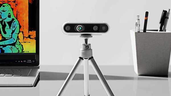
Three popular alternatives offer distinctly different tradeoffs. The “Been Around The Block” name is Occipital, with their more expensive Structure Pro sensor. The “Old Name, New Face” option is Microsoft Azure Kinect, the latest non-gaming-focused successor to the gaming peripheral that started it all. And let’s not forget OAK-D as the “New Kid On The Block” that started with a crowdfunding campaign and building an user community by doing things like holding contests. Each of these will appeal to a different niche, and we’ll keep our eye open in the future. Let’s see if any of them find the success that eluded the original Kinect, Google’s Tango, and now Intel’s RealSense.
[via Engadget]