Transform Kicad Design To Patchwork For Isolation Routing

Tuning a desktop router and your board designs for isolation routing can be a bit tricky, with thin traces usually being the first victim. For simple prototype boards you usually don’t need tightly packed traces, you just want to isolate the nets. To do this with a minimum amount of routing, [Michael Schembri] created kicad-laser-min, a command-line utility that takes a Kicad PCB design and expands all the tracks and pads to their maximum possible width.

Laser scribed PCB with maximum track widths

The software takes one layer of the PCB layout, converts it to black and white, and then runs a C++ Voronoi algorithm on it to dilate each track and pad until it meets another expanding region. Each region is colourised, and OpenCV edge detection is used to produce the contours that need to be milled or etched. A contour following algorithm is then used to create the G-code. The header image shows the output of each step.

Full source code is available on GitHub. [Michael] has had good results with his own boards, which are scribed using a laser cutter before etching, but welcomes testing and feedback from other users. He has found that OpenCV doesn’t always completely close all the contours, but the gaps are usually smaller than the engraving width of his laser, so no shorts are created.

This is basically “Scribble style” prototyping with CAD and CNC tools. If you prefer scribe and etch, you might consider building a simple PCB shaker for faster etching. If you have a router but want to avoid the dust, you can use a carbide scribe to scratch out the tracks without needing to etch.

Designing 3D Printed Enclosures For KiCad PCBs

If you’ve used KiCad before, you’re certainly familiar with the handy 3D view that shows you a rendered view of what your assembled board would look like. But as [Vadim Panov] explains, you can take this capability a step further. With a few extra tools and a little bit of know-how, you can leverage KiCad’s PCB renderings to make custom 3D printable enclosures.

The first step is to design the PCB as you normally would in KiCad. This could be an original PCB of your own invention, or a digital representation of an off-the-shelf model you want to build an enclosure for. If the latter, then the PCB doesn’t need to be 100% accurate; the goal is really just to get the big components into roughly the right areas so you can get the clearances right. Though obviously you’ll want to make sure the board’s outer dimensions and mounting hole locations are recreated as accurately as possible.

From there, [Vadim] recommends a tool called StepUp. This will take your PCB KiCad PCB files and create either a STEP or STL file of the assembled board which can be imported into your CAD package of choice. For the purposes of this demonstration he’s sticking with FreeCAD, as he likes the idea of it being a completely FOSS toolchain from start to finish.

Now that you have a model of the PCB in your CAD software, the rest is up to you. Naturally, there are existing enclosure models you can use such as the ones produced by the “Ultimate Box Maker” that we covered previously, but you could just as easily start building a new enclosure around the digital PCB.

Looking for a bit more guidance? As it so happens, our very own [Anool Mahidharia] will be presenting a class on how you can develop a KiCad + FreeCAD workflow as part of our recently launched HackadayU initiative.

Tidy Laser Cut Packaging For PCBs With KiCAD

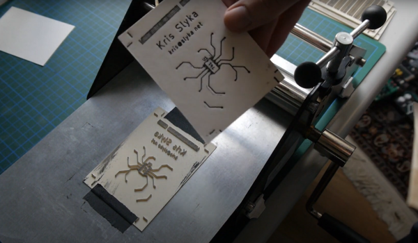
A laser cutter is a useful tool to have in any workshop. While many hackers use them for their cutting abilities, it’s important to remember that they can be great as engravers, too. [Wrickert] was well aware of this when he set his to work, producing attractive packaging for his Tindie orders.

[Wrickert] sells a variety of small PCB-based devices on Tindie, and it’s nice to have something to package them up with, rather than just sending a bare board. To do this quickly and effectively, KiCAD is used to help generate the packaging from the original PCB geometry itself. The board outlines are exported as an SVG file, reopened in KiCAD, and then used to create the required cardboard parts. The laser can then also be used to engrave the cardboard too.

It’s a tidy packaging solution that requires no messy inks or printers, and can be designed in the same software as the device itself. We’ve covered this area before, talking about what it takes to go from a home project to a saleable kit. If you’re in the game, you might find [Wrickert]’s hack to be just the ticket!

KiCad Panelization Made Easy

There’s a new Python-based script that will panelize your KiCad circuit boards from the command line. The project by [Jan Mrázek] is called KiKit and works on .kicad_pcb files to arrange them in a grid with your choice of mousebites or v-cuts for separating the boards after production.

When working with smaller boards it’s common practice to group them together into panels. This is done to speed up PCB assembly as multiple boards can have solder paste applied, go through a pick and place machine, and be sent into the reflow oven as a single unit. Often this is done manually, but in many cases this script will save you the time while delivering the results you need.

Let’s say you really wanted to make a whole bunch of those Xling open source Tamagotchi-like key fobs we saw a couple of weeks back. Using KiKit you can gang up six of the boards at a time, using “mousebites” to keep them together during production but make it easy to separate them after all the components are soldered:

/usr/local/bin/kikit panelize grid --space 3 --gridsize 2 3 --tabwidth 3 --tabheight 3 --htabs 2 --vtabs 1 --mousebites 0.5 1 0.25 --radius 1 Xling/hardware/xling.kicad_pcb xling_panel.kicad_pcb

You can see that the parameters let you set space between the boards, number of boards in the grid, width of the tabs, tab dimensions, number of tabs between boards, and even the radius of the curve where the tabs meet the board. These settings were pulled from the examples page, which demonstrates outcomes for many different settings options.

If you want to give this a try, we suggest installing directly from the repository, as improvements are ongoing and the pip3 version didn’t have all of the options shown in the examples. For us this was as easy as sudo python3 setup.py install and then calling the script with the full path /usr/local/bin/kikit.

Results from this board are both impressive and cautionary. You can see the top edge of the design is recessed yet the most up-to-date version of KiKit was still able to make the connection. However, how this affects the USB connector on the bottom of the board design may be something to consider before pulling the trigger on your panel order.

Altium Has Its 2kicad Moment

Around these parts we tend to be exponents of the KiCad lifestyle; what better way to design a PCBA than with free and open source tools that run anywhere? But there are still capabilities in commercial EDA packages that haven’t found their way into KiCad yet, so it may not always be the best tool for the job. Altium Designer is a popular non-libre option, but at up to tens of thousands of USD per seat it’s not always a good fit for users and businesses without a serious need.

It’s hard to find an exciting photo of a dialog box

What do you do as a KiCad user who encounters a design in Altium you’d like to work with? Well as of April 3rd 2020, [Thomas Pointhuber] has merged the beginnings of a native Altium importer into KiCad which looks to be slated for the 6.0 release. As [Thomas] himself points out in the patch submission, this is hardly the first time a 3rd party Altium importer has been published. His new work is a translation of the Perl plugin altium2kicad by [thesourcerer8]. And back in January another user left a comment with links to four other (non-KiCad) tools to handle Altium files.

If you’d like to try out this nifty new feature for yourself, CNX has a great walkthrough starting at building KiCad from source. As for documents to test against the classic BeagleBone Black sources seen above can be found at on GitHub. Head past the break to check out the very boring, but very exciting video of the importer at work, courtesy of [Thomas] himself. We can’t wait to give this a shot!

Thanks for the tip [Chris Gammell]!

Continue reading “Altium Has Its 2kicad Moment”

Can Solder Paste Stencils Be 3D Printed? They Can!

3D printed solder paste stencil, closeup.

[Jan Mrázek]’s  success with 3D printing a solder paste stencil is awfully interesting, though he makes it clear that it is only a proof of concept. There are a lot of parts to this hack, so let’s step through them one at a time.

First of all, it turns out that converting a PCB solder paste layer into a 3D model is a bit of a challenge. A tool [Jan] found online didn’t work out, so he turned to OpenSCAD and wrote a script (available on GitHub) which takes two DXF files as input: one for the board outline, and one for the hole pattern. If you’re using KiCad, he has a Python script (also on GitHub) which will export the necessary data.

The result is a 3D model that is like a solder paste mask combined with a raised border to match the board outline, so that the whole thing self-aligns by fitting on top of the PCB. A handy feature, for sure. [Jan] says the model pictured here printed in less than 10 minutes. Workflow-wise, that certainly compares favorably to waiting for a stencil to arrive in the mail. But how do the actual solder-pasting results compare?

3D printed solder stencil on PCB, after applying solder paste.

[Jan] says that the printed stencil had a few defects but it otherwise worked fine for 0.5 mm pitch ICs and 0402 resistors, and the fact that the 3D printed stencil self-registered onto the board was a welcome feature. That being said, it took a lot of work to get such results. [Jan]’s SLA printer is an Elegoo Mars, and he wasn’t able to have it create holes for 0.2 mm x 0.5 mm pads without first modifying his printer for better X/Y accuracy.

In the end, he admits that while a functional DIY solder stencil can be 3D printed in about 10 minutes, it’s not as though professionally-made stencils that give better results are particularly expensive or hard to get. Still, it’s a neat trick that could come in handy. Also, a quick reminder that we stepped through how to make a part in OpenSCAD in the past, which should help folks new to OpenSCAD make sense of [Jan]’s script.

DeepPCB Routes Your KiCAD PCBs

Computers can write poetry, even if they can’t necessarily write good poetry. The same can be said of routing PC boards. Computers can do it, but can they do it well? Of course, there are multiple tools each with pluses and minuses. However, a slick web page recently announced deeppcb.ai — a cloud-based AI router — and although details are sparse, there are a few interesting things about the product.

First, it supports KiCAD. You provide a DSN file, and within 24 hours you get a routed SES file. Maybe. You get three or four free boards –apparently each week — after which there is some undisclosed fee. Should you just want to try it out, create an account (which is quick and free — just verify your e-mail and create a password). Then in the “Your Boards” section there are a few examples already worked out.

Continue reading “DeepPCB Routes Your KiCAD PCBs”