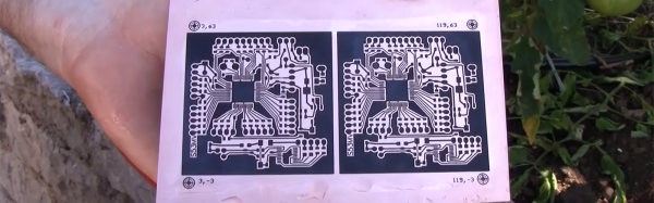
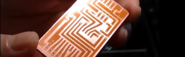
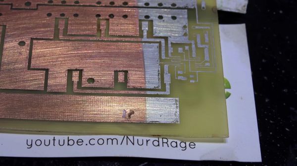
Chemotransfer For DIY PCBs

Making PCBs with the toner transfer method has been around since you could buy your traces at Radio Shack. There are a million techniques for removing copper from sheets of fiberglass, from milling to using resist pens, to the ubiquitous laser printer toner transfer. Here’s a technique we haven’t seen before. [Darko Volk] is calling this ‘chemotransfer’. It’s mostly a laser printer toner transfer process, but the toner is transferred from paper to copper with the help of a special mix of solvents.

This chemotransfer process is almost identical to the usual process of making a toner transfer PCB. First, the design is printed in reverse on dextrin-coated paper, the paper is placed down on polished copper, the entire assembly is sent through a laminator, and finally the board is etched with the chemical of your choice. The key difference here is a solvent applied to the copper just before the design is laid down. [Darko Volk] made a mixture of 25% “cleaning petrol” (benzene, naphtha, or gasoline, or some sort of light hydrocarbon, apparently), 5% linseed oil, and 70% isopropanol. This apparently aids in releasing the toner from the paper and sticking it down to the copper.

From there, the process is effectively a standard toner transfer process. [Darko Volk] is using a solution of sodium persulphate for the etch, and rigged a camera up to a CNC machine for the drilling.

This process can be expanded to two-layer boards very easily using a light table to align the layers of paper before placing them down on the copper. You can check out a video of the fabrication of a single side and double sided board below.

Thanks [Andrej] for the tip.

Continue reading “Chemotransfer For DIY PCBs”

Why Not Expose Your PCBs Through An LCD?

Most people who have dabbled in the world of electronic construction will be familiar in some form with the process of producing a printed circuit board by exposing a UV sensitive coating through a transparent mask, before moving on to etching. Older readers will have created their masks by hand with crêpe paper tape on acetate, while perhaps younger ones started by laser-printing from their CAD package.

How about a refinement of the process, one which does away with the acetate mask entirely? [Ionel Ciobanuc] may have the answer, in the form of an exposure through an LCD screen. The video below the break shows how it’s done, starting with a (probably a bit too lengthy) sequence on applying the photo-resist coating to the board, and then sitting LCD on top of UV lamp with the board positioned at the top of the pile.

It’s an interesting demonstration, and one that certainly removes a step in the process of PCB creation as it brings the pattern direct from computer to board without an intermediate. Whether or not it’s worth the expenditure on an LCD is up to you, after all a sheet of acetate is pretty cheap and if you already have a laser printer you’re good to go. We’re curious to know whether or not any plastic components in the LCD itself might be damaged by long-term exposure to intense UV light.

Continue reading “Why Not Expose Your PCBs Through An LCD?”

The Art Of Blinky Business Cards

Business cards are stuck somewhere between antiquity and convenience. On one hand, we have very convenient paperless solutions for contact swapping including Bluetooth, NFC, and just saying, “Hey, put your number into my phone, please.” On the other hand, holding something from another person is a more personal and memorable exchange. I would liken this to the difference between an eBook and a paperback. One is supremely convenient while the other is tactile. There’s a reason business cards have survived longer than the Rolodex.

Protocols and culture surrounding the exchange of cards are meant to make yourself memorable and a card which is easy to associate with you can work long after you’ve given your card away. This may seem moot if you are assigned cards when you start a new job, but personal business cards are invaluable for meeting people outside of work and you are the one to decide how wild or creative to make them.

Continue reading “The Art Of Blinky Business Cards”

Customizable PCB Business Card

[Corey Harding] designed his business card as a USB-connectable demonstration of his skill. If potential manager inserts the card in a USB drive, open a text editor, then touches the copper pad on the PCB, [Corey]’s contact info pops up in the text box.

In addition to working as a business card, the PCB also works as a Tiny 85 development board, with a prototyping area for adding sensors and other components, and with additional capabilities broken out: you can add an LED, and there’s also room for a 1K resistor, a reset button, or break out the USB’s 5V for other uses. There’s an AVR ISP breakout for reflashing the chip.

Coolly, [Corey] intended for the card to be an Open Source resource for other people to make their own cards, and he’s providing the Fritzing files for the PCB. Fritzing is a great program for beginning and experienced hardware hackers to lay out quick and dirty circuits, make wiring diagrams, and even export PCB designs for fabrication. You can download [Corey]’s files from his GitHub repository.

For another business card project check out this full color business card we published last month.

Hackaday Prize Entry: A PCB To Emulate Coin Cells

The Coin Cell Emulator CR2016/CR2032 by [bobricius] homes in on a problem some hardware developers don’t realize they have: when working on hardware powered by the near-ubiquitous CR2016 or CR2032 format 3V coin cells, power can be a bit troublesome. Either the device is kept fed with coin cells as needed during development, or the developer installs some breakout wires to provide power from a more convenient source.

[bobricius]’s solution to all this is a small PCB designed to be inserted into most coin cell holders just like the cell itself. It integrates a micro USB connector with a 3V regulator for using USB as an external power source. The board also provides points for attaching alligator clips, should one wish to conveniently measure current consumption. It’s a tool with a purpose, and cleverly uses the physical shape of the PCB itself as an integral part of the function, much like another of [bobricius]’s projects: the Charlieplexed 7-segment LED display.

The Components Are INSIDE The Circuit Board

Through-hole assembly means bending leads on components and putting the leads through holes in the circuit board, then soldering them in place, and trimming the wires. That took up too much space and assembly time and labor, so the next step was surface mount, in which components are placed on top of the circuit board and then solder paste melts and solders the parts together. This made assembly much faster and cheaper and smaller.

Now we have embedded components, where in order to save even more, the components are embedded inside the circuit board itself. While this is not yet a technology that is available (or probably even desirable) for the Hackaday community, reading about it made my “holy cow!” hairs tingle, so here’s more on a new technology that has recently reached an availability level that more and more companies are finding acceptable, and a bit on some usable design techniques for saving space and components.

Continue reading “The Components Are INSIDE The Circuit Board”

How To Do PCB Art In Eagle

Last month I had the pleasure of creating a new piece of hardware for Tindie. [Jasmine], the queen bee of Tindie, and I designed, developed, and kitted three hundred Tindie badges in ten days leading up to DEF CON. The badges were a complete success, they introduced soldering to a lot of people, and were loved by all.

This badge was such a rousing success, it’s now official Tindie swag. We’ll be handing out a few of these blinky badges at upcoming events. But as of right now we’ve already handed out our entire stock, that means we need to build more. The second run meant ordering a thousand PCBs.

We could just do another run, and order a few more PCBs from the Gerbers I’ve already designed. I’m not really happy with the first version of this badge, though, and this is an opportunity to improve my design. This also gives me an opportunity to demonstrate my workflow for creating artistic boards in Eagle.

Effectively, what I’ll be demonstrating here is the creation of the Benchoff Nickel. A few months ago, [Andrew Sowa] took a portrait of yours truly, changed the colors to what is available on a normal OSHPark PCB, and turned that into different layers in KiCad. There are a few differences here. Firstly, I’ll be using a blue solder mask, although the same technique can be applied to green, red, yellow, white, or black soldermask. Secondly, this is Eagle, and I’m going to do the majority of the work with a BMP import. This is the fast and easy way to do things; if you want a KiCad tutorial, check out [Andrew]’s work, or my overly-involved multiple silkscreen process for KiCad. I don’t recommend this overly-involved process if you can help it. It took 20 hours to do the art for my previous project in KiCad, and I estimate it would have taken two in Eagle.

With that said, here’s the easy, cheap, and fast way of doing artistic boards in Eagle.

Continue reading “How To Do PCB Art In Eagle”