Opening Up ASIC Design

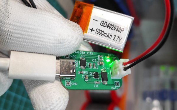
The odds are that if you’ve heard about application-specific integrated circuits (ASICs) at all, it’s in the context of cryptocurrency mining. For some currencies, the only way to efficiently mine them anymore is to build computers so single-purposed they can’t do anything else. But an ASIC is a handy tool to develop for plenty of embedded applications where efficiency is a key design goal. Building integrated circuits isn’t particularly straightforward or open, though, so you’ll need some tools to develop them such as OpenRAM.

Designing the working memory of a purpose-built computing system is a surprisingly complex task which OpenRAM seeks to demystify a bit. Built in Python, it can help a designer handle routing models, power modeling, timing, and plenty of other considerations when building static RAM modules within integrated circuits. Other tools for taking care of this step of IC design are proprietary, so this is one step on the way to a completely open toolchain that anyone can use to start building their own ASIC.

This tool is relatively new and while we mentioned it briefly in an article back in February, it’s worth taking a look at for anyone who needs more than something like an FPGA might offer and who also wants to use an open-source tool. Be sure to take a look at the project’s GitHub page for more detailed information as well. There are open-source toolchains if you plan on sticking with your FPGA of choice, though.

Copy And Paste Lithium Battery Protection

Lithium batteries have, nearly single-handedly, ushered in the era of the electric car, as well as battery energy storage of grid power and plenty of other technological advances not possible with older battery chemistries. There’s just one major downside: these lithium cells can be extremely finicky. If you’re adding one to your own project you’ll have to be extremely careful to treat them exactly how they are designed to be treated using something like this boilerplate battery protection circuit created by [DIY GUY Chris].

The circuit is based around the TP4056 integrated circuit, which handles the charging of a single lithium cell — in this design using supplied power from a USB port. The circuit is able to charge a cell based on the cell’s current charge state, temperature, and a model of the cell. It’s also paired with a DW01A chip which protects the cell from various undesirable conditions such as over-current, overcharge, and over-voltage.

The best thing about this design isn’t the design itself, but that [DIY GUY Chris] built the circuit schematic specifically to be easily copied into PCB designs for other projects, which means that lithium batteries can more easily be integrated directly into his other builds. Be sure to check out our primer on how to deal with lithium batteries before trying one of your own designs, though.

Continue reading “Copy And Paste Lithium Battery Protection”

Comparing Solar Energy Harvesters

There doesn’t have to be much more to setting up a simple solar panel installation than connecting the panel to a battery. Of course we would at least recommend the use of a battery management system or charge controller to avoid damaging the battery, although in a pinch it’s not always strictly necessary. But these simple systems leave a lot on the table, and most people with any sizable amount of solar panels tend to use a maximum power point tracking (MPPT) system to increase the yield of the panels. For a really tiny installation like [Salvatore] has, you’ll want to take a look at a similar system known as a solar energy harvester.

[Salvatore] is planning to use an energy harvester at his small weather station, which is currently powered by an LDO regulator and a small solar cell. While this is fairly energy efficient, the energy harvesters that he is testing with this build will go far beyond what an LDO is capable of. The circuit actually has two energy harvesters built onto it which allows him to test the capabilities of both before he makes a decision for his weather station. Every amount of energy is critical when using the cell he has on hand, which easily fits in the palm of one’s hand.

The testing of this module isn’t complete yet, but he does have two working prototypes to test in future videos to see which one truly performs the best. For a project of this size, this is a great way to get around the problem of supplying a small amount of power to something remote. For a larger solar panel installation, you’ll definitely want to build an MPPT system though.

Continue reading “Comparing Solar Energy Harvesters”

Integrated Circuit Manufacturing At Bell Labs In 1983

With the never ending march of technological progress, arguably the most complex technologies become so close to magic as to be impenetrable to those outside the industry in which they operate. We’ve seen walkthrough video snapshots of just a small part of the operation of modern semiconductor fabs, but let’s face it, everything you see is pretty guarded, hidden away inside large sealed boxes for environmental control reasons, among others, and it’s hard to really see what’s going on inside.

Let’s step back in time a few decades to 1983, with an interesting tour of the IC manufacturing facility at Bell Labs at Murray Hill (video, embedded below) and you can get a bit more of an idea of how the process works, albeit at a time when chips hosted mere tens of thousands of active devices, compared with the countless billions of today. This fab operates on three inch wafers, producing about 100 die each, with every one handled and processed by hand whereas modern wafers are much bigger, die often much smaller with the total die per wafer in the thousands and are never handled by a filthy human.

Particle counts of 100 per cubic foot might seem laughable by modern standards, but device geometries back then were comparatively large and the defect rate due to it was not so serious. We did chuckle somewhat seeing the operator staff all climb into their protective over suits, but open-faced with beards-a-plenty poking out into the breeze. Quite simply, full-on bunny suits were simply not necessary. Anyway, whilst the over suits were mostly for the environment, we did spot the occasional shot of an operator wearing some proper protective face shielding when performing some of the higher risk tasks, such as wafer cleaning, after all as the narrator says “these acids are strong enough to eat through the skin” and that would certainly ruin your afternoon.

No story about integrated circuit processing would be complete without mentioning the progress of [Sam Zeloof] and his DIY approach to making chips, and whilst he’s only managing device counts in the hundreds, this can only improve given time.

Continue reading “Integrated Circuit Manufacturing At Bell Labs In 1983”

Old Printer Becomes Direct Laser Lithography Machine

What does it take to make your own integrated circuits at home? It’s a question that relatively few intrepid hackers have tried to answer, and the answer is usually something along the lines of “a lot of second-hand equipment.” But it doesn’t all have to be cast-offs from a semiconductor fab, as [Zachary Tong] shows us with his homebrew direct laser lithography setup.

Most of us are familiar with masked photolithography thanks to the age-old process of making PCBs using photoresist — a copper-clad board is treated with a photopolymer, a mask containing the traces to be etched is applied, and the board is exposed to UV light, which selectively hardens the resist layer before etching. [Zach] explores a variation on that theme — maskless photolithography — as well as scaling it down considerably with this rig. An optical bench focuses and directs a UV laser into a galvanometer that was salvaged from an old laser printer. The galvo controls the position of the collimated laser beam very precisely before focusing it on a microscope that greatly narrows its field. The laser dances over the surface of a silicon wafer covered with photoresist, where it etches away the resist, making the silicon ready for etching and further processing.

Being made as it is from salvaged components, aluminum extrusion, and 3D-printed parts, [Zach]’s setup is far from optimal. But he was able to get some pretty impressive results, with features down to 7 microns. There’s plenty of room for optimization, of course, including better galvanometers and a less ad hoc optical setup, but we’re keen to see where this goes. [Zach] says one of his goals is homebrew microelectromechanical systems (MEMS), so we’re looking forward to that.

Continue reading “Old Printer Becomes Direct Laser Lithography Machine”

The decapped chip on top of some other DIP IC, with magnet wire soldered to the die, other ends of the magnet wire soldered to pins of the "body donor" DIP IC.

Factory Defect IC Revived With Sandpaper And Microsoldering

We might be amidst a chip shortage, but if you enjoy reverse-engineering, there’s never a shortage of intriguing old chips to dig into – and the 2513N 5×7 character ROM is one such chip. Amidst a long thread probing a few of these (Twitter, ThreadReader link), [TubeTime] has realized that two address lines were shorted inside of the package. A Twitter dopamine-fueled quest for truth has led him to try his hand at making the chip work anyway. Trying to clear the short with an external PSU led to a bond wire popping instead, as evidenced by the ESD diode connection disappearing.

A dozen minutes of sandpaper work resulted in the bare die exposed, making quick work of the bond wires as a side effect. Apparently, having the bond pads a bit too close has resulted in a factory defect where two of the pads merged together. No wonder the PSU wouldn’t take that on! Some X-acto work later, the short was cleared. But without the bond wires, how would [TubeTime] connect to it? This is where the work pictured comes in. Soldering to the remains of the bond wires has proven to be fruitful, reviving the chip enough to continue investigating, even if, it appears, it was never functional to begin with. The thread continued on with comparing ROMs from a few different chips [TubeTime] had on hand and inferences on what could’ve happened that led to this IC going out in the wild.

Such soldering experiments are always fun to try and pull off! We rarely see soldering on such a small scale, as thankfully, it’s not always needed, but it’s a joy to witness when someone does IC or PCB microsurgery to fix factory defects that render our devices inoperable before they were even shipped. Each time that a fellow hacker dares to grind the IC epoxy layers down and save a game console or an unidentified complex board, the world gets a little brighter. And if you aren’t forced to do it for repair reasons, you can always try it in an attempt to build the smallest NES in existence!

Continue reading “Factory Defect IC Revived With Sandpaper And Microsoldering”

The Zeloof Z2 Intergrated Circuit Has 100 Transistors

Back in 2018 we reported on the first silicon integrated circuit to be produced in a homemade chip fab. It was the work of [Sam Zeloof], and his Z1 chip was a modest six-transistor amplifier. Not one to rest on his laurels, he’s back with another chip, this time the Z2 is a hundred-transistor array. The Z2 occupies about a quarter of the area of the previous chip and uses a 10µm polysilicon gate process as opposed to the Z1’s metal gates. It won’t solve the global chip shortage, but this is a major step forward for anyone interested in building their own semiconductors.

The transistors themselves are FETs, and [Sam] is pleased with their consistency and characteristics. He’s not measured his yield on all samples, but of the twelve chips made he says he has one fully functional chip and a few others with at least 80% functionality. The surprise is that his process is less complex than one might expect, which he attributes to careful selection of a wafer pre-treated with the appropriate oxide layer.

You can see more about the Z2 in the video below the break. Meanwhile, should you wish to learn more about the Z1 you can see [Sam’s] Hackaday Superconference talk on the subject. We’re looking forward to the Z3 when it eventually arrives, with bated breath!

Continue reading “The Zeloof Z2 Intergrated Circuit Has 100 Transistors”