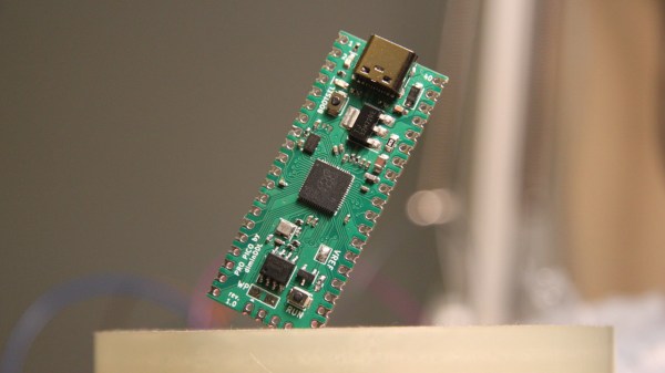
Ever feel like the Pi Pico board could be doing way more given its footprint? Does it bother you that the RP2040’s ADC quality is even further decreased because of the noisy onboard switching regulator? Miffed about decisions like the MicroUSB socket, the 2MB flash, or lack of the reset button? [Dmytro] brings us an open-source Pi Pico design, sporting the same RP2040 and a fully compatible footprint, but adding a number of improvements to its surroundings.
There’s a good few additions, all of them hacker-friendly – [Dmytro] adds comfortably-spaced reset and boot buttons, a USB-C socket, a dedicated low-noise voltage reference for the ADC, one more LED, and an I2C EEPROM footprint socket that is compatible with FRAM chips. Everything worth preserving is preserved – the pinout stays the same, including the SWD connector, which now sports an extra RESET pin. The bottom side USB testpoints remain, with only the four testpoints changed for more useful signals. Last but not least, the switching regulator is replaced by the venerable 1117 – you lose the ability to power your Pico from two AAs, and the capacitor series resistor requirement isn’t great, but you can easily put one of the drop-in 1117 replacement regulators on there.
What’s great is that the design is fully open-source, with KiCad files available. Want to design your own Pi Pico footprint board, improve upon this one even further, or maybe make a more tailored one? Treat yourself to the GitHub repository! There’s also a pinout diagram and a KiCanvas schematic for all your tinkering needs. We’ve covered drop-in replacements for classic drawer-inhabiting parts like the Pi Zero, for the 7805 (twice!), the 6502 CPU, and even for the DE9 serial port connector. No matter the purpose, they’re always a joy to see.
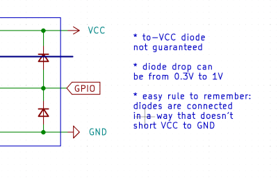 Thankfully, in modern-day Western climates and with modern tech, you are not likely to encounter ESD-caused problems, but they were way more prominent back in the day. For instance, older hackers will have stories of how FETs were more sensitive, and touching the gate pin mindlessly could kill the FET you’re working with. Now, we’ve fixed this problem, in large part because we have added ESD-protective diodes inside the active components most affected.


