A while ago, [Eric Strebel] created a backpack hanger. The result was great — by just bolting this backpack hanger to the wall, he kept his backpack off the floor and out of the way. There was even a place for him to set his phone to charge. [Eric] is thinking about turning this idea into a product, and just posted a video on his process of making a cardboard mockup.
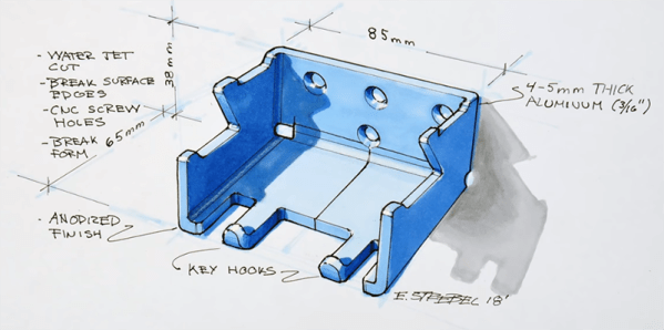
Since this is a study in industrial design, any mockup will need to keep in mind how the finished article will be constructed. In this case, [Eric] is going to use 4-5mm thick aluminum, cut on a water jet, bent into place, and finally anodized. The finished product will be made out of bent sheet aluminum, so this little bit of product design will use Matboard — a thick, heavy cardboard often used for mounting pictures in frames. The Matboard will substitute for the aluminum, as it is carefully cut, bent, and glued into shape.
The tools for this build are simple, just a hobby knife, razor blade, ruler, and a pen. But there are a few tricks to working with Matboard. To bend these pieces perfectly, [Eric] is painting one side with water. This loosens the fibers in the Matboard, allowing for perfect creases before one layer of the build is glued together.
Once a few layers of this Matboard are glued together, the finished product becomes less like cardboard and more like a very soft wood. This allows [Eric] to use belt sanders and countersink drill bits to give a little bit of polish to this one-off prototype. This finished article works great, and now [Eric] is looking at taking this idea into production.