It’s fair to say that the majority of Hackaday readers have not built any hardware that’s slipped the surly bonds of Earth and ventured out into space proper. Sure we might see the occasional high altitude balloon go up under the control of some particularly enterprising hackers, but that’s still a far cry from a window seat on the International Space Station. Granted the rapid commercialization of space has certainly added to that exclusive group of space engineers over the last decade or so, but something tells us it’s still going to be quite some time before we’re running space-themed hacks with the regularity of Arduino projects.
That being the case, you might assume the protocols and methods used to develop a scientific payload for the ISS must seem like Latin to us lowly hackers. Surely any hardware that could potentially endanger an orbiting outpost worth 100+ billion dollars, to say nothing of the human lives aboard it, would utilize technologies we can hardly dream of. It’s probably an alphabet soup of unfamiliar acronyms up there. After all, this is rocket science, right?
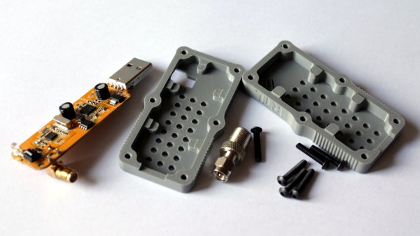
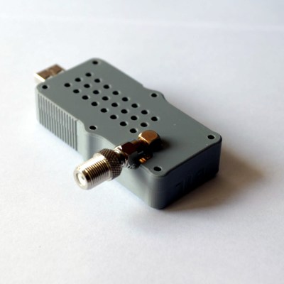
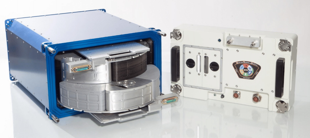
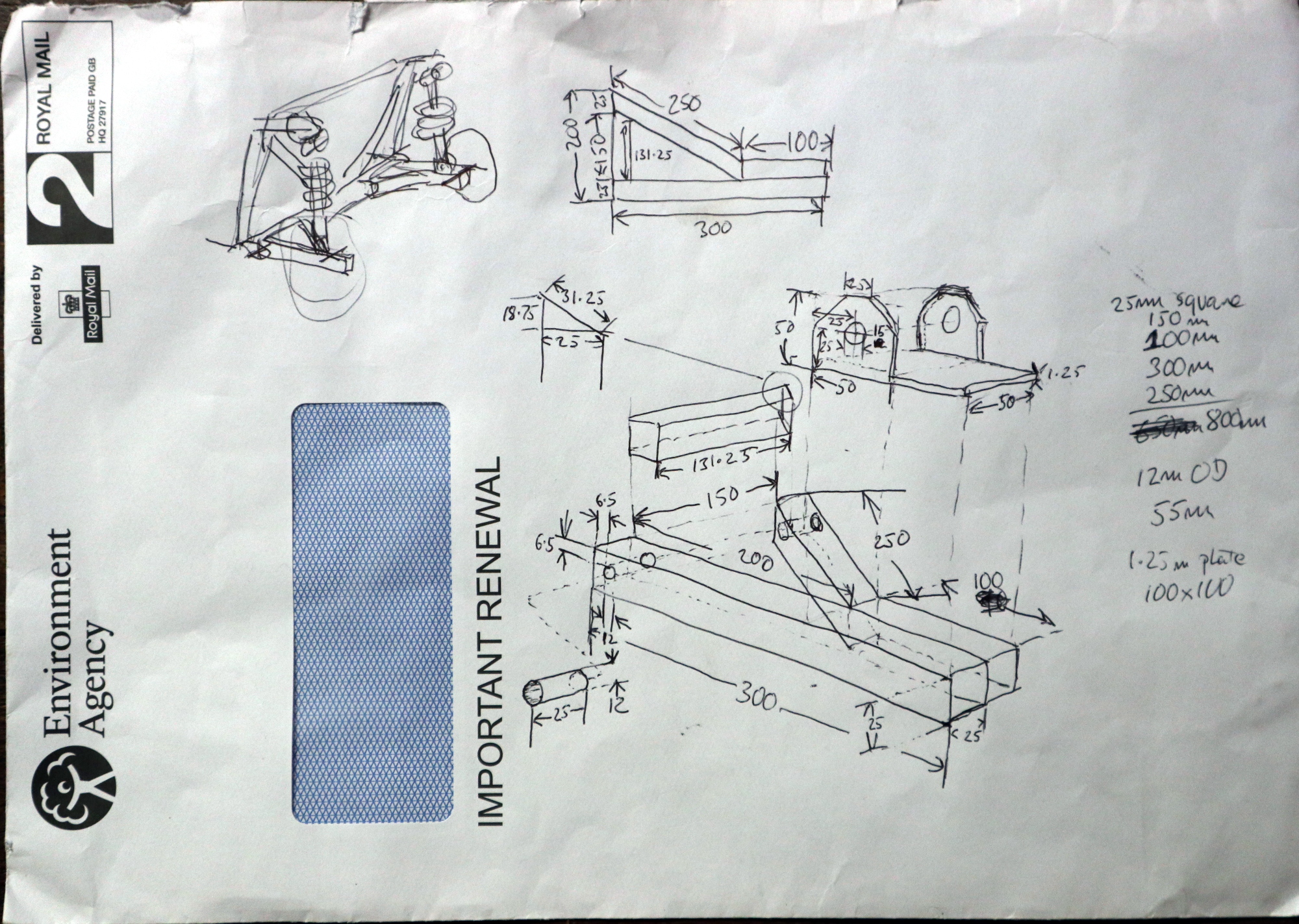
There’s certainly an element of truth in there someplace, as hardware that gets installed on the Space Station is obviously held to exceptionally high standards. But Brad Luyster is here to tell you that not everything up there is so far removed from our Earthly engineering. In fact, while watching his 2018 Hackaday Superconference talk “Communication, Architecture, and Building Complex Systems for SPAAACE”, you might be surprised just how familiar it all sounds. Detailing some of the engineering that went into developing the Multi-use Variable-G Platform (MVP), the only centrifuge that’s able to expose samples to gravitational forces between 0 and 1 g, his talk goes over the design considerations that go into a piece of hardware for which failure isn’t an option; and how these lessons can help us with our somewhat less critically important projects down here.
Check out Brad’s newly published talk video below, and then join me after the break for a look at the challenges of designing hardware that will live in space.
Continue reading “The Thrill Of Building Space Hardware To Exceptionally High Standards”
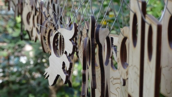
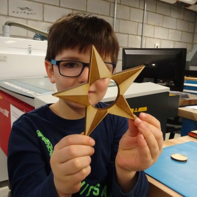 It all began when the kids were taken to a local fab lab at the École Polytechnique and made some laser-cut napkin holders from plywood for personal use. Later, they decided to design, manufacture, and sell them at the Ottawa Maker Faire. Money for the plywood came from piggy banks, 23 different designs made the cut, and a total of 103 rings were made. A display board and signs made from reclaimed materials rounded out the whole set.