“Don’t worry, that’ll buff right out.” Alarming news this week as the James Webb Space Telescope team announced that a meteoroid had hit the space observatory’s massive primary mirror. While far from unexpected, the strike on mirror segment C3 (the sixth mirror from the top going clockwise, roughly in the “south southeast” position) that occurred back in late May was larger than any of the simulations or test strikes performed on Earth prior to launch. It was also not part of any known meteoroid storm in the telescope’s orbit; if it had been, controllers would have been able to maneuver the spacecraft to protect the gold-plated beryllium segments. The rogue space rock apparently did enough damage to be noticeable in the data coming back from the telescope and to require adjustment to the position of the mirror segment. While it certainly won’t be the last time this happens, it would have been nice to see one picture from Webb before it started accumulating hits.
die57 Articles
Electronic Dice Is Introduction To Microcontroller Programming
By now most of us are familiar with the Arduino platform. It’s an inexpensive and fairly easy way into the world of microcontrollers. For plenty of projects, there’s no need to go beyond that unless you have a desire to learn more of the inner workings of microcontrollers in general. [Cristiano] was interested in expanding some of his knowledge, so he decided to build this electronic dice using a PIC microcontroller instead of the Arduino platform he was more familiar with.
As a result, this project is set up as a how-to for others looking to dive further into the world of microcontrollers that don’t have the same hand-holding setup as the Arduino. To take care of the need for a random number for the dice, the PIC’s random number generator is used but with the added randomness of a seed from an internal timer. The timer is started when a mercury tilt switch signals the device that it has been rolled over, and after some computation a single digit number is displayed on a seven-segment display.
While it might seem simple on the surface, the project comes with an in-depth guide on programming the PIC family of microcontrollers, and has a polish not normally seen on beginner projects, including the use of the mercury tilt switch which gives it a retro vibe. For some other tips on how to build projects like this, take a look at this guide on how to build power supplies for your projects as well.
Continue reading “Electronic Dice Is Introduction To Microcontroller Programming”
Factory Defect IC Revived With Sandpaper And Microsoldering
We might be amidst a chip shortage, but if you enjoy reverse-engineering, there’s never a shortage of intriguing old chips to dig into – and the 2513N 5×7 character ROM is one such chip. Amidst a long thread probing a few of these (Twitter, ThreadReader link), [TubeTime] has realized that two address lines were shorted inside of the package. A Twitter dopamine-fueled quest for truth has led him to try his hand at making the chip work anyway. Trying to clear the short with an external PSU led to a bond wire popping instead, as evidenced by the ESD diode connection disappearing.
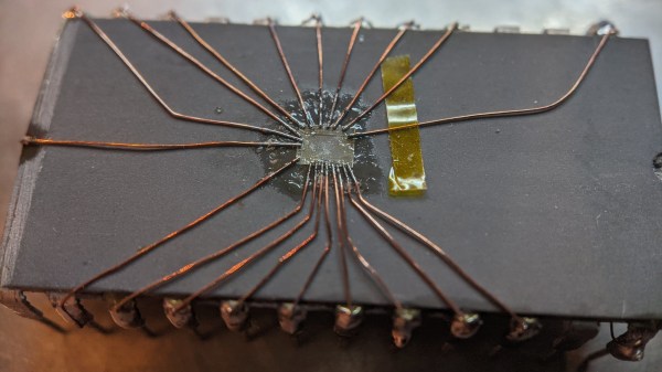
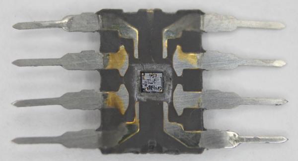
A dozen minutes of sandpaper work resulted in the bare die exposed, making quick work of the bond wires as a side effect. Apparently, having the bond pads a bit too close has resulted in a factory defect where two of the pads merged together. No wonder the PSU wouldn’t take that on! Some X-acto work later, the short was cleared. But without the bond wires, how would [TubeTime] connect to it? This is where the work pictured comes in. Soldering to the remains of the bond wires has proven to be fruitful, reviving the chip enough to continue investigating, even if, it appears, it was never functional to begin with. The thread continued on with comparing ROMs from a few different chips [TubeTime] had on hand and inferences on what could’ve happened that led to this IC going out in the wild.
Such soldering experiments are always fun to try and pull off! We rarely see soldering on such a small scale, as thankfully, it’s not always needed, but it’s a joy to witness when someone does IC or PCB microsurgery to fix factory defects that render our devices inoperable before they were even shipped. Each time that a fellow hacker dares to grind the IC epoxy layers down and save a game console or an unidentified complex board, the world gets a little brighter. And if you aren’t forced to do it for repair reasons, you can always try it in an attempt to build the smallest NES in existence!
Continue reading “Factory Defect IC Revived With Sandpaper And Microsoldering”
555 Teardown Isn’t Just A Good Time, It’s To Die For
It seems only appropriate that hot on the heels of the conclusion of Hackaday’s 555 Timer Contest that [Ken Shirriff] posts a silicon die teardown of an early version of a hacker’s favorite chip, the 555.
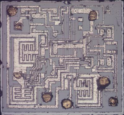
Starting with a mystery chip from January 1973, [Eric Schlaepfer] painstakingly sanded down the package to reveal the die, which he deemed to be a 555 timer. Why didn’t they know it was a 555 timer to start? Because the package was not marked with “555” but rather some other marks that you can see in the blog post.
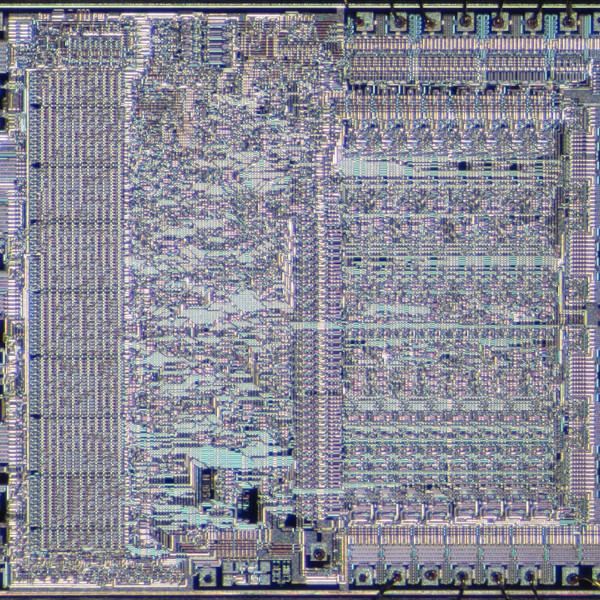
In addition to a great explanation of how the 555 works in general, [Ken] has taken a microscopic look at the 555 die itself. The schematic of a 555 is easily available, and [Ken] identifies not just sections of the die but individual components. He goes further yet by explaining how the PNP and NPN resistors are constructed in silicon. There’s also a nice and juicy bit of insight into the resistors in the IC, but we won’t spoil it here.
Be sure to show your love for the winners of the 555 contest, or at the very least check out the project that took the stop spot: a giant sized 555 that you don’t need a microscope to see inside of.
Retrotechtacular: The Drama Of Metal Forming
It may seem overwrought, but The Drama of Metal Forming actually is pretty dramatic.
This film is another classic of mid-century corporate communications that was typically shown in schools, which the sponsor — in this case Shell Oil — seeks to make a point about the inevitable march of progress, and succeeds mainly in showing children and young adults what lay in store for them as they entered a working world that needed strong backs more than anything.
Despite the narrator’s accent, the factories shown appear to be in England, and the work performed therein is a brutal yet beautiful ballet of carefully coordinated moves. The sheer power of the slabbing mills at the start of the film is staggering, especially when we’re told that the ingots the mill is slinging about effortlessly weigh in at 14 tons apiece. Seeing metal from the same ingots shooting through the last section of a roller mill at high speed before being rolled into coils gives one pause, too; the catastrophe that would result if that razor-sharp and red-hot metal somehow escaped the mill doesn’t bear imagining. Similarly, the wire drawing process that’s shown later even sounds dangerous, with the sound increasing in pitch to a malignant whine as the die diameter steps down and the velocity of the wire increases.
There are the usual charming anachronisms, such as the complete lack of safety gear and the wanton disregard for any of a hundred things that could instantly kill you. One thing that impressed us was the lack of hearing protection, which no doubt led to widespread hearing damage. Those were simpler times, though, and the march of progress couldn’t stop for safety gear. Continue reading “Retrotechtacular: The Drama Of Metal Forming”
Decapping Components Hack Chat With John McMaster
Join us on Wednesday, March 10 at noon Pacific for the Decapping Components Hack Chat with John McMaster!
We treat them like black boxes, which they oftentimes are, but what lies beneath the inscrutable packages of electronic components is another world that begs exploration. But the sensitive and fragile silicon guts of these devices can be hard to get to, requiring destructive methods that, in the hands of a novice, more often than not lead to the demise of the good stuff inside.
To help us sort through the process of getting inside components, John McMaster will stop by the Hack Chat. You’ll probably recognize John’s work from Twitter and YouTube, or perhaps from his SiliconPr0n.org website, home to beauty shots of some of the chips he has decapped. John is also big in the reverse engineering community, organizing the Mountain View Reverse Engineering meetup, a group that meets regularly to discuss the secret world of components. Join us as we talk to John about some of the methods and materials used to get a look inside this world.
 Our Hack Chats are live community events in the Hackaday.io Hack Chat group messaging. This week we’ll be sitting down on Wednesday, March 10 at 12:00 PM Pacific time. If time zones have you tied up, we have a handy time zone converter.
Click that speech bubble to the right, and you’ll be taken directly to the Hack Chat group on Hackaday.io. You don’t have to wait until Wednesday; join whenever you want and you can see what the community is talking about.
Continue reading “Decapping Components Hack Chat With John McMaster”
Open-DIP Surgery Cuts Retro Chips Down To Size
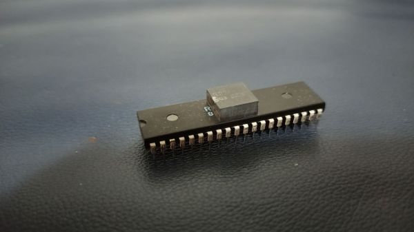
At least by today’s standards, some of the early chips were really, really big. They may have been revolutionary and they certainly did shrink the size of electronic devices, but integrating a 40-pin DIP into a modern design can be problematic. The solution: cut off all the extra plastic and just work with the die within.
 Continue reading “Open-DIP Surgery Cuts Retro Chips Down To Size”


