Silicon Photolithography The PCB Way

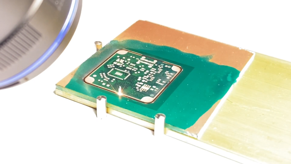
[ProjectsInFlight] has been doing some fantastic work documenting his DIY semiconductor fab lately. Next up: exploring down-and-dirty photolithography methods.

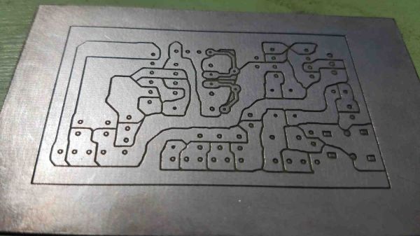
If you’ve been following along with this series — and why wouldn’t you? — you’ll recall [ProjectsInFlight]’s earlier experiments, like creating oxide layers on silicon chips with a homebrew tube furnace and exploring etchants that can selectively remove them. But just blasting away the oxide layer indiscriminately isn’t really something you need to do when etching the fine features needed to fabricate a working circuit. The trouble is, most of the common photoresist solutions used by commercial fabs are unobtainium for hobbyists, leading to a search for a suitable substitute.

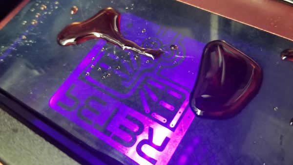
Surprisingly, PCB photoresist film seemed to work quite well, but not without a lot of optimization by [ProjectsInFlight] to stick it to the silicon using a regular laminator. Also in need of a lot of tweaking was the use of a laser printer to create masks for the photolithography process on ordinary transparency film, including the surprisingly effective method of improving the opacity of prints with acetone vapor. There were also extensive experiments to determine the best exposure conditions, a workable development process, and the right etchants to use. Watch the video below for a deep dive into all those topics as well as the results, which are pretty good.

There’s a lot to be said for the methodical approach that [ProjectsInFlight] is taking here. Every process is explored exhaustively, with a variety of conditions tested before settling on what works best. It’s also nice to see that pretty much all of this has been accomplished with the most basic of materials, all of which are easily sourced and pretty cheap to boot. We’re looking forward to more of the same here, as well as to see what others do with this valuable groundwork.

Continue reading “Silicon Photolithography The PCB Way”

JavaScript App Uses Advanced Math To Make PCBs Easier To Etch

We all remember the litany from various math classes we’ve taken, where frustration at a failure to understand a difficult concept bubbles over into the classic, “When am I ever going to need to know this in real life?” But as we all know, even the most esoteric mathematical concepts have applications in the real world, and failure to master them can come back to haunt you.

Take Voronoi diagrams, for example. While we don’t recall being exposed to these in any math class, it turns out that they can be quite useful in a seemingly unrelated area: converting PCB designs into easy-to-etch tessellated patterns. Voronoi diagrams are in effect a plane divided into different regions, or “cells”, each centered on a “seed” object. Each cell is the set of points that are closer to a particular seed than they are to any other seed. For PCBs the seeds can be represented by the traces; dividing the plane up into cells around those traces results in a tessellated pattern that’s easily etched.

To make this useful to PCB creators, [Craig Iannello] came up with a JavaScript application that takes an image of a PCB, tessellates the traces, and spits out G-code suitable for a laser engraver. A blank PCB covered with a layer of spray paint, the tessellated pattern is engraved into the paint, and the board is etched and drilled in the usual fashion. [Craig]’s program makes allowances for adding specific features to the board, like odd-shaped pads or traces that need specific routing.

This isn’t the first time we’ve seen Voronoi diagrams employed for PCB design, but the method looks so easy that we’d love to give it a try. It even looks as though it might work for CNC milling of boards too.

Laser Blasts Out High-Quality PCBs

With how cheap and how fast custom PCBs have gotten, it almost doesn’t make sense to roll your own anymore, especially when you factor in the messy etching steps and the less than stellar results. That’s not the only way to create a PCB, of course, and if you happen to have access to a 20-Watt fiber laser, you can get some fantastic homemade PCBs that are hard to tell from commercial boards.

Lucikly, [Saulius Lukse] of Kurokesu fame has just such a laser on hand, and with a well-tuned toolchain and a few compromises, he’s able to turn out 0.1-mm pitch PCBs in 30 minutes. The compromises include single-sided boards and no through-holes, but that should still allow for a lot of different useful designs. The process starts with Gerbers going through FlatCAM and then getting imported into EZCAD for the laser. There’s a fair bit of manual tweaking before the laser starts burning away the copper between the traces, which took about 20 passes for 0.035-mm foil on FR4. We have to admit that watching the cutting proceed in the video below is pretty cool.

Once the traces are cut, UV-curable solder resist is applied to the whole board. After curing, the board goes back to the laser for another pass to expose the pads. A final few passes with the laser turned up to 11 cuts the finished board free. We wonder why the laser isn’t used to drill holes; we understand that vias would be hard to connect to the other side, but it seems like through-hole components could be supported. Maybe that’s where [Saulius] is headed with this eventually, since there are traces that terminate in what appears to be via pads.

Whatever the goal, these boards are really slick. We usually see lasers used to remove resist prior to traditional etching, so this is a nice change.

Continue reading “Laser Blasts Out High-Quality PCBs”

Put That New Resin Printer To Work Making PCBs

With all the cool and useful parts you can whip up (relatively) quickly on a 3D printer, it’s a shame you can’t just print a PCB. Sure, ordering a PCB is quick, easy, and cheap, but being able to print one-offs would peg the needle on the instant gratification meter.

[Peter Liwyj] may just have come up with a method to do exactly that. His Instructables post goes into great detail about his method, which uses an Elegoo Mars resin printer and a couple of neat tricks. First, a properly cleaned board is placed copper-side down onto a blob of SLA resin sitting on the print bed. He tricks the printer into thinking the platform is all the way down for the first layer by interrupting the photosensor used to detect home. He lets the printer go through one layer of an STL file that contains his design, which polymerizes a thin layer of plastic onto the copper. The excess resin is wiped gently away and the board goes straight into a ferric chloride etching bath. The video below shows the whole process.

As simple as it sounds, it looks like it works really well. And [Peter] didn’t just stumble onto this method; he approached it systematically and found what works best. His tips incude using electrical tape as a spacer to lift the copper off the print surface slightly, cleaning the board with Scotchbrite rather than sandpaper, and not curing the resin after printing. His toolchain is a bit uncoventional — he used SketchUp to create the traces and exported the STL. But there are ways to convert Gerbers to STLs, so your favorite EDA package can probably fit in to the process too.

Don’t have a resin printer? Don’t worry — FDM printers can work too.

Continue reading “Put That New Resin Printer To Work Making PCBs”

PCB Finishes Hack Chat

Join us on Wednesday, March 11 at noon Pacific for the PCB Finishes Hack Chat with Mark Hughes and Elijah Gracia!

There’s no way to overestimate the degree to which the invention of the printed circuit board revolutionized electronics. What was once the work of craftspeople weaving circuits together with discrete components, terminal strips, and wiring harnesses could now be accomplished with dedicated machines, making circuit construction an almost human-free process. And it was all made possible by figuring out how to make copper foil stick to a flat board, and how to remove some of it while leaving the rest behind.

​Once those traces are formed, however, there’s more work to be done. Bare copper is famously reactive stuff, and oxides soon form that will make the traces difficult to solder later. There are hundreds of different ways to prevent this, and PCB surface finishing has become almost an art form itself. Depending on the requirements for the circuit, traces can be coated with tin, lead, gold, nickel, or any combination of the above, using processes ranging from electroplating to immersion in chemical baths. And the traces aren’t the only finishes; solder resist and silkscreening are both important to the usability and durability of the finished board.

For this Hack Chat, we’ll be talking to Elijah Gracia and Mark Hughes from Royal Circuit Solutions. They’re both intimately familiar with the full range of PCB coatings and treatments, and they’ll help us make sense of the alphabet soup​: HASL, OSP, ENIG, IAg, LPI, and the rest. We’ll learn what the different finishes do, which to choose under what circumstances, and perhaps even learn a bit about how to make our homebrew boards look a little more professional and perform a bit better.

join-hack-chatOur Hack Chats are live community events in the Hackaday.io Hack Chat group messaging. This week we’ll be sitting down on Wednesday, March 11 at 12:00 PM Pacific time. If time zones have got you down, we have a handy time zone converter.

Click that speech bubble to the right, and you’ll be taken directly to the Hack Chat group on Hackaday.io. You don’t have to wait until Wednesday; join whenever you want and you can see what the community is talking about.

CNC Machine Most Satisfyingly Mills Double-Sided PCBs

We know that by this point in the development of CNC technology, nothing should amaze us. We’ve seen CNC machines perform feats of precision that shouldn’t be possible, whether it be milling a complex jet engine turbine blade or just squirting out hot plastic. But you’ve just got to watch this PCB milling CNC machine go through its paces!

The machine is from an outfit called WEGSTR, based in the Czech Republic. While it appears to be optimized for PCB milling and drilling, the company also shows it milling metals, wood, plastic, and even glass. The first video below shows the machine milling 0.1 mm traces in FR4; the scale of the operation only becomes apparent when a gigantic toothbrush enters the frame to clear away a little swarf. As if that weren’t enough, the machine then cuts traces on the other side of the board; vias created by filling drilled holes with copper rivets and peening them over with a mandrel and a few light hammer taps connect the two sides.

Prefer your boards with solder resist and silkscreening? Not a problem, at least judging by the second video, which shows a finished board getting coated with UV-cure resist and then having the machine mill away just the resist on the solder pads. We’re not sure how they deal with variations in board thickness or warping, but they sure have it dialed in. Regardless of how they optimized the process, it’s a pleasure to watch.

At about $2,600, these are not cheap machines, but they may make sense for someone needing high-quality boards with rapid turnaround. And who’s to say a DIY machine couldn’t do as good a job? We’ve seen plenty of them before, and covered the pros and cons of etching versus milling too.

Continue reading “CNC Machine Most Satisfyingly Mills Double-Sided PCBs”

Amiga Repairs Put One Tough Little Machine Back In Service

Returning a piece of retro hardware to factory condition is generally a labor of love for the restorationist. A repair, on the other hand, is more about getting a piece of equipment back into service. But the line between repair and restoration is sometimes a fine one, with the goals of one bleeding over into the other, like in this effort to save an otherwise like-new Amiga 2000 with a leaky backup battery.

Having previously effected emergency repairs to staunch the flow of electrolyte from the old batteries and prevent further damage, [Retromat] entered the restoration phase of the project. The creeping ooze claimed several caps and the CPU socket as it spread across the PCB, but the main damage was to the solder resist film itself. In the video below you can clearly see flaky, bubbly areas in the mask where the schmoo did its damage.

Using a fiberglass eraser, some isopropyl alcohol, and far more patience than we have, [Retromat] was able to remove the damaged resist to reveal the true extent of the damage below. Thankfully, most of the traces were still intact; only a pair of lines under the CPU socket peeled off as he was removing it. After replacing them with fine pieces of wire, replacing the corroded caps and socket, and adding a coin-cell battery holder to replace the old battery, the exposed traces were coated with a varnish to protect them and the machine was almost as good as new.

Amigas were great machines in their day and launched more than one business. They’ve proved their staying power too, some even in mission-critical roles.

Continue reading “Amiga Repairs Put One Tough Little Machine Back In Service”