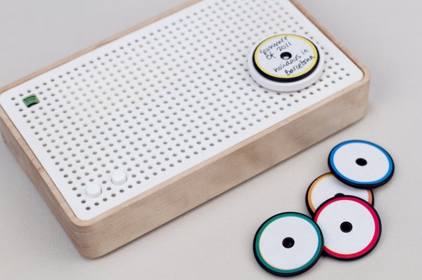
Otters Deliver A High Power Stationary Audio Experience

Our favorite raft of otters is back at it again with another display of open source audio prowess as they bring us the OtterCastAmp, the newest member of the OtterCast family of open source audio multitools. If you looked at the previous entry in the series – the OtterCastAudio – and thought it was nice but lacking in the pixel count or output power departments then this is the device for you.

The Amp is fundamentally a very similar device to the OtterCastAudio. It shares the same Allwinner S3 Cortex-A application processor and runs the same embedded Linux build assembled with Buildroot. In turn it offers the same substantial set of features and audio protocol support. It can be targeted by Snapcast, Spotify Connect or AirPlay if those are your tools of choice, or act as a generic PulseAudio sink for your Linux audio needs. And there’s still a separate line in so it source audio as well.

One look at the chassis and it’s clear that unlike the OtterCastAudio this is not a simple Chromecast Audio replacement. The face of the OtterCastAmp is graced by a luscious 340×800 LCD for all the cover art your listening ear can enjoy. And the raft of connectors in the back (and mountain of inductors on the PCBA) make it clear that this is a fully fledged class D amplifier, driving up to 120W of power across four channels. Though it may drive a theoretical 30W or 60W peak across its various outputs, with a maximum supply power of 100W (via USB-C power delivery, naturally) the true maximum output will be a little lower. Rounding out the feature set is an Ethernet jack and some wonderfully designed copper PCB otters to enjoy inside and out.

As before, it looks like this design is very close to ready for prime time but not quite there yet, so order at your own risk. Full fab files and some hints are linked in the repo mentioned above. If home fabrication is a little much it looks like there might be a small manufacturing run of these devices coming soon.

The ARMv9 ISA, And What It Can Do For You

The number of distinct ARM Instruction Set Architectures (ISA) versions has slowly increased, with Arm adding a new version every few years. The oldest ISA version in common use today is ARMv6, with the ARMv6 ISA (ARM11) found in the original Raspberry Pi SBC and Raspberry Pi Zero (BCM2835). The ARMv6 ISA was introduced in 2002, followed by ARMv7 in 2005 (start of Cortex-A series) and ARMv8 in 2011. The latter was notable for adding 64-bit support.

With ARMv7 being the first of the Cortex cores, and ARMv8 adding 64-bit support in the form of AArch64, what notable features does ARMv9 bring to the table? As announced earlier this year, ARMv9’s focus appears to be on adding a whole host of features that should improve vector processing (vector extensions, or SVE) as well as digital signal processing (DSP) and security, with its Confidential Compute Architecture (CCA).

In addition to this, ARMv9 also includes all of the features that were added with ARMv8.1, v8.2, v8.3 and so on. In essence, this makes an ARMv9-based processor theoretically capable of going toe-to-toe with the best that Intel and AMD have to offer.

Continue reading “The ARMv9 ISA, And What It Can Do For You”

Forth Module The Size Of A Stick Of Gum

Australian engineer [John Catsoulis] developed a small module called the Scamp2 dedicated to running Forth. The focus of his Udamonic project was not only to highlight Forth, but to make a module which was easy to use and doesn’t require any IDE on your computer. According to the website, these modules have found their niche in education as well as rapid prototyping for product development. His site has some good resources, including several Scamp/Forth example applications such as a model train controller or adding a real-time clock module.

The core of the module is a Microchip PIC24F64GB202 MCU with 64K Flash and 8K RAM. Of this, Forth takes up only 20K of Flash and 2K of RAM. [John] is using FlashForth, a version of Forth which came from [Mikael Nordman] at the University of Queensland almost ten years ago. FlashForth has been implemented on a wide variety of PIC and AVR ATmega processors and has apparently developed quite a following in Australia and elsewhere.

We estimate from the photo that the Scamp is about 80 mm long, just slightly longer than a standard piece of MIL-A-A-20175A Type II chewing gum ( 73 mm ). You can use it as-is, or with the header pins installed, the Scamp can be plugged into a breadboard for easy hacking. Regarding the interfacing of Scamp to other equipment, [John] says “Writing software to use other hardware is very easy, and fun.” We like his attitude.

Here is some more information from his Hackaday.io project page, and he also has a Tindie site. If you want a good overview of using Forth in embedded systems, check out Forth: The Hacker’s Language by our own Forth-guru [Elliot Williams]. Thanks to [Stephen Walters] for sending in the tip.

Continue reading “Forth Module The Size Of A Stick Of Gum”

[Ken Shirriff] Picks Apart Mystery Chip From Twitter Photo

It’s no secret that the work of [Ken Shirriff] graces the front pages of Hackaday quite frequently. He’s back again, this time reverse engineering a comparator chip from a photo on Twitter. The mysterious chip was decapped, photographed under a microscope, and subsequently posted on the internet with an open call to figure out what it did.

[Ken] stepped up, and at first glance, it was obvious that most of the chip is unused, and there appeared to be four copies of the same circuit. After identifying resistors and the different transistor types, [Ken] found differential pairs.

Differential pairs form the heart of most op-amps, and by chaining them together, you can get a strong enough signal to treat it as a logic signal. Based on the design and materials, [Ken] estimates the chip is from the 1970s. Given that it appears to be ECL (Emitter-Coupled Logic), it could just be four comparators. But there are still a few things that don’t add up as two comparators have additional inverted outputs. Searching the part number offered few if any clues, so this will remain somewhat a mystery.

We’ve covered [Ken’s] incredible chip sleuthing before here, such as the Sharp EL-8 from 1969.

A HALO Of LEDs For Every Ear

Few things get a Hackaday staffer excited like bunches of tiny LEDs. The smaller and denser the better, any form will do as long as we can get a macro shot or a video of a buttery smooth animation. This time we turn to [Sawaiz Syed] and [Open Kolibri] to deliver the brightly lit goods with the minuscule HALO 90 reactive LED earrings.

The HALO 90’s are designed to work as earrings, though we suspect they’d make equally great brooches, hair accessories, or desk objects. To fit this purpose each one is a minuscule 24 mm in diameter and weighs a featherweight 5.2 grams with the CR2032 battery (2.1 g for the PCBA alone). Functionally their current software includes three animation modes, each selectable via a button on device; audio reactive, halo (fully lit), and sparkle. Check out the documentation for details on expected battery life in each mode, but suffice to say that no matter what these earrings will make it through a few nights out.

In terms of hardware, the HALO 90’s are as straightforward as you’d expect. Each device is driven by an STM8 at its maximum 16MHz which is more than fast enough to keep the 90 charliplexed 0402 LEDs humming along at a 1kHz update rate, even with realtime audio processing. In fact the BOM here is refreshingly simple with just 8 components; the LEDs, microcontroller and microphone, battery holder and passives, and the button. [Sawaiz] even designed an exceptionally slick case to go with each pair of earrings, which holds two HALO 90’s with two CR2032’s and includes a magnetic closure for the most satisfying lid action possible.

As with some of his other work, [Sawaiz] has produced a wealth of exceptional documentation to go with the HALO 90’s. They’re available straight from him fully assembled, but with documentation this good the path to a home build should be well lit and accessible. He’s even chosen parts with an eye towards long availability, low cost, and ease of sourcing so no matter when you decide to get started it should be a snap.

It was difficult to choose just a few images from [Sawaiz]’s mesmerizing collection, so if you need more feast your eyes on the expanded set after the break.

Continue reading “A HALO Of LEDs For Every Ear”

WiFive55: More Than A Smart 555 Replacement

“You could’ve done that with a 555 timer.” But what if all you have on hand is an ESP8266? [TechColab] needed to control a solenoid valve with a short pulse via a solid-state relay (SSR) but found that the trusty 555 timer was tricky to set properly. Additionally, they wanted to add features, such as fixed pulse length, that were difficult to implement—even with multiple timers. Still wanting to keep things cheap and accessible, [TechColab] has created the WiFive55, a 555 replacement based on the ESP-01 ESP8266 board.

[TechColab] began by investigating existing ESP-01 solid-state relay boards but found that many of them momentarily enable the output on startup—a risk [TechColab] deemed unacceptable. This was resolved in the WiFive55 by adding an RC filter to the SSR output, eliminating the output glitches at the cost of slowing switching time to around 20 ms—an acceptable trade for many SSR applications.

Since they were going to design a new PCB to support this improved ESP-01 SSR controller, [TechColab] decided to go all-out. To support loads of widely varying sizes, the PCB supports an optoisolator that switches up to 1 A, a MOSFET that switches up to 2 A, and an on-board relay or SSR that can switch up to 3 A. For heavy loads, it includes connections for an off-board SSR, which allow it to switch whatever current the SSR can handle (easily over 50 A). Because the ESP-01 is slightly more capable than the 555, the WiFive55 supports control via WiFi, GPIO, serial, and push-button. Keeping with the WiFive55’s original role as a 555 replacement, it even includes a header exposing a 555-like trigger and output interface!

We always like seeing inexpensive boards like the ESP-01 being used to their full potential, and we can’t wait to see what software [TechColab] cooks up for this! If you’re interested in getting started with the ESP-01, you might consider starting with this guide to blinking an LED over WiFi.

Logic Chip Teardown From Early 1990s IBM ES/9000 Mainframe

The 1980s and early 1990s were a bit of an odd time for semiconductor technology, with the various transistor technologies that had been used over the decades slowly making way for CMOS technology. The 1991-vintage IBM ES/9000 mainframe was one of the last systems to be built around bipolar transistor technology, with [Ken Shirriff] tearing into one of the processor modules (TCM) that made up one of these mainframes.

A Thermal Conduction Module from an IBM ES/9000 mainframe.

Five of these Thermal Conduction Modules (127.5 mm a side) made up the processor in these old mainframes. Most of note are the use of the aforementioned bipolar transistors and the use of DCS-based (differential current switch) logic. With the already power-hungry bipolar transistors driven to their limit in the ES/9000, and the use of rather massive DCS gates, each TCM was not only fed many amperes of electricity, but also capable of dissipating up to 600 Watts of power.

Each TCM didn’t contain a single large die of bipolar transistors either, but instead many smaller dies were bonded on a specially prepared ceramic layer in which the wiring was added through a very precise process. While an absolute marvel of engineering, the ES/9000 was essentially a flop, and by 1997 IBM too would move fully to CMOS transistor technology.

Over the years we’ve featured a lot of [Ken]’s work, perhaps you’d like to know more about his techniques.