When one thinks of applications for 3D printing, optical components don’t seem to be a good fit. With the possible exception of Fresnel lenses, FDM printing doesn’t seem up to the job of getting the smooth surfaces and precision dimensions needed to focus light. Resin printing might be a little closer to the mark, but there’s still a long way to go between a printed blank and a finished lens.
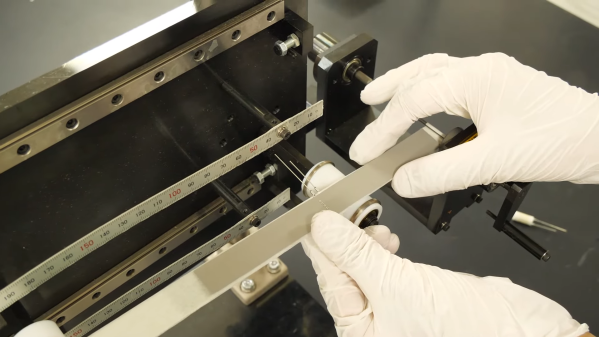
That gap is what [Fraens] aims to fill with this homebrew lens grinding machine. It uses the same basic methods used to grind and polish lenses for centuries, only with printed components and lens blanks. The machine itself consists of a motorized chuck for holding the lens blank, plus an articulated arm to hold the polishing tool. The tool arm has an eccentric drive that wobbles the polishing tool back and forth across the blank while it rotates in the chuck. Lens grinding requires a lot of water and abrasive, so a large bowl is provided to catch the swarf and keep the work area clean.
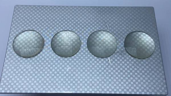
Lens blanks are printed to approximately their finished dimensions using clear resin in an SLA printer. [Fraens] spent a lot of time optimizing the printing geometry to minimize the number of print layers required. He found that a 30° angle between the lens and the resin pool worked best, resulting in the clearest blanks. To polish the rough blanks, a lapping tool is made from polymer modeling clay; after baking it dry, the tool can hold a variety of pads and polishing compounds. From there it’s just a matter of running the blank through a range of abrasives to get the desired final surface.
Are the lenses fantastic? Well, they’re probably not going to make it into fine optical equipment, but they’re a lot better than you might expect. Of course, there’s plenty of room for improvement; better resins might result in clearer blanks, and perhaps degassing the uncured resin under vacuum might help with bubbles. Skipping the printed blanks and going with CNC-machined acrylic might be worth a try, too.
Continue reading “A 3D Printed Grinder For Printed Lens Blanks”
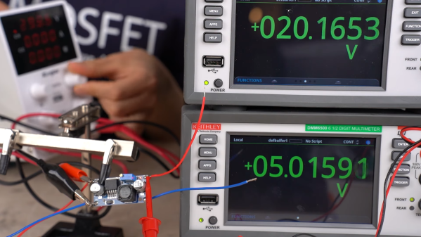
 Or do you? It’s not so clear after watching [Denki Otaku]’s video on a bargain bag of buck converters he got from Amazon — ¥1,290 for a lot of ten, or $0.85 a piece. The thing that got [Denki]’s Spidey senses tingling is the chip around which these boards were built: the LM2596. These aren’t especially cheap chips; Mouser lists them for about $5.00 each in a reel of 500.