Art With Technology Hack Chat

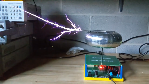
Join us on Wednesday, June 16 at noon Pacific for the Art with Technology Hack Chat with Cory Collins!

As hackers, we naturally see the beauty of technology. We often talk in terms of the aesthetics of a particular hack, or the elegance of one solution over another, and we can marvel at the craftsmanship involved in everything from a well-designed PCB to a particularly clever reverse-engineering effort. Actually using technology to create art is something that’s often harder for us to appreciate, though, and looking at technological art from the artist’s side can be pretty instructive.

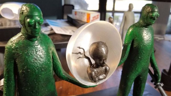
Cory Collins is an animator and artist with a long history of not only putting tech to work to create art, but also using it as the subject of his pieces. Cory’s work has brought life to video games, movies, and TV shows for years; more recently, he has turned his animation skills to developing interactive educational material for medical training. He has worked in just about every physical and digital medium imaginable, and the characters and scenes he has created are sometimes whimsical, sometimes terrifying, but always engaging.

Cory will stop by the Hack Chat to talk about what he has learned about technology from the artist’s perspective. Join us as we dive into the creative process, look at how art influences technology and vice versa, and learn how artistic considerations can help us address the technical problems every project eventually faces.

join-hack-chatOur Hack Chats are live community events in the Hackaday.io Hack Chat group messaging. This week we’ll be sitting down on Wednesday, June 16 at 12:00 PM Pacific time. If time zones have you tied up, we have a handy time zone converter.

Click that speech bubble to the right, and you’ll be taken directly to the Hack Chat group on Hackaday.io. You don’t have to wait until Wednesday; join whenever you want and you can see what the community is talking about.

A Smart Light Bulb Running Doom Is A Pretty Bright Idea

A light bulb might seem like an unlikely platform for gaming, but we’re living in the future now, so anything is possible. And with enough know-how, it turns out that an RGB light bulb can indeed be modified to run Doom.

[Ed note: The project pages and video got pulled right when this went to press. Nicola received a takedown notice.  We’ll let you know more when we do. The main link has been updated to the Wayback Machine.]

That’s not to say that the Ikea TRÅDFRI light bulb is the only thing [Nicola Wrachien] needed to accomplish the hack. But the bulb, specifically this addressable GU10 RGB LEB bulb, donated the most critical component, a Silicon Labs MGM210L wireless microcontroller, with enough processing power to run vanilla Doom. Added to the microcontroller was a TFT display, a controller made from a handful of buttons and a shift register, and a few odds and ends to stitch it all together. Some more memory was needed, though, so [Nicola] used an 8 MB QSPI flash memory and a couple of neat tricks to reduce latency and improve bandwidth. There are a lot of neat tricks with this one, but the coolest thing might just be that the whole footprint of the build isn’t that much bigger than the original bulb. Check out the surprisingly smooth gameplay in the video below.

This is a nice addition to the seemingly neverending “Will it Doom?” series. We’ve seen the classic game ported to everything from a GPS to a kitchen “bump bar” computer and even to an oscilloscope.

Continue reading “A Smart Light Bulb Running Doom Is A Pretty Bright Idea”

Digital X-Ray Scanner Teardown Yields Bounty Of Engineering Goodies

We’ll just go ahead and say it right up front: we love teardowns. Ripping into old gear and seeing how engineers solved problems — or didn’t — is endlessly fascinating, even for everyday devices like printers and radios. But where teardowns really get interesting is when the target is something so odd and so specialized that you wouldn’t normally expect to get a peek at the outside, let alone tramp through its guts.

[Mads Barnkob] happened upon one such item, a Fujifilm FCR XG-1 digital radiography scanner. The once expensive and still very heavy piece of medical equipment was sort of a “digital film system” that a practitioner could use to replace the old-fashioned silver-based films used in radiography, without going all-in on a completely new digital X-ray suite. It’s a complex piece of equipment, the engineering of which yields a lot of extremely interesting details.

The video below is the third part of [Mads]’ series, where he zeroes in on the object of his desire: the machine’s photomultiplier tube. The stuff that surrounds the tube, though, is the real star, at least to us; that bent acrylic light pipe alone is worth the price of admission. Previous videos focused on the laser scanner unit inside the machine, as well as the mechatronics needed to transport the imaging plates and scan them. The video below also shows experiments with the PM tube, which when coupled with a block of scintillating plastic worked as a great radiation detector.

We’ve covered a bit about the making of X-rays before, and a few of the sensors used to detect them too. We’ve also featured a few interesting X-ray looks inside of tech, from a Starlink dish to knock-off adapters.

Continue reading “Digital X-Ray Scanner Teardown Yields Bounty Of Engineering Goodies”

Hackaday Links Column Banner

Hackaday Links: June 13, 2021

When someone offers to write you a check for $5 billion for your company, it seems like a good idea to take it. But in the world of corporate acquisitions and mergers, that’s not always the case, as Altium proved this week when they rebuffed a A$38.50 per share offer from Autodesk. Altium Ltd., the Australian company whose flagship Altium Designer suite is used by PCB and electronic designers around the world, said that the Autodesk offer “significantly undervalues” Altium, despite the fact that it represents a 42% premium of the company’s share price at the end of last week. Altium’s rejection doesn’t close the door on ha deal with Autodesk, or any other comers who present a better offer, which means that whatever happens, changes are likely in the EDA world soon.

There were reports this week of a massive explosion and fire at a Chinese polysilicon plant — sort of. A number of cell phone videos have popped up on YouTube and elsewhere that purport to show the dramatic events unfolding at a plant in Xinjiang province, with one trade publication for the photovoltaic industry reporting that it happened at the Hoshine Silicon “997 siloxane” packing facility. They further reported that the fire was brought under control after about ten hours of effort by firefighters, and that the cause is under investigation. The odd thing is that we can’t find a single mention of the incident in any of the mainstream media outlets, even five full days after it purportedly happened. We’d have figured the media would have been all over this, and linking it to the ongoing semiconductor shortage, perhaps erroneously since the damage appears to be limited to organic silicone production as opposed to metallic silicon. But the company does supply something like 17% of the world’s supply of silicon metal, so anything that could potentially disrupt that should be pretty big news.

It’s always fun to see “one of our own” take a project from idea to product, and we like to celebrate such successes when they come along. And so it was great to see the battery-free bicycle tire pressure sensor that Hackaday.io user CaptMcAllister has been working on make it to the crowdfunding stage. The sensor is dubbed the PSIcle, and it attaches directly to the valve stem on a bike tire. The 5-gram sensor has an NFC chip, a MEMS pressure sensor, and a loop antenna. The neat thing about this is the injection molding process, which basically pots the electronics in EDPM while leaving a cavity for the air to reach the sensor. The whole thing is powered by the NFC radio in a smartphone, so you just hold your phone up to the sensor to get a reading. Check out the Kickstarter for more details, and congratulations to CaptMcAllister!

We’re saddened to learn of the passing of Dale Heatherington last week. While the name might not ring a bell, the name of his business partner Dennis Hayes probably does, as together they founded Hayes Microcomputer Products, makers of the world’s first modems specifically for the personal computer market. Dale was the technical guru of the partnership, and it’s said that he’s the one who came up with the famous “AT-command set”. Heatherington only stayed with Hayes for seven years or so before taking his a $20 million share of the company and retiring, which of course meant more time and resources to devote to tinkering with everything from ham radio to battle bots. ATH0, Dale.

Macro Model Makes Atomic Force Microscopy Easier To Understand

For anyone that’s fiddled around with a magnifying glass, it’s pretty easy to understand how optical microscopes work. And as microscopes are just an elaboration on a simple hand lens, so too are electron microscopes an elaboration on the optical kind, with electrons and magnets standing in for light and lenses. But atomic force microscopes? Now those take a little effort to wrap your brain around.

Luckily for us, [Zachary Tong] over at the Breaking Taps YouTube channel recently got his hands on a remarkably compact atomic force microscope, which led to this video about how AFM works. Before diving into the commercial unit — but not before sharing some eye-candy shots of what it can do — [Zach] helpfully goes through AFM basics with what amounts to a macro version of the instrument.

His macro-AFM uses an old 3D-printer as an X-Y-Z gantry, with a probe head added to the printer’s extruder. The probe is simply a sharp stylus on the end of a springy armature, which is excited into up-and-down oscillation by a voice coil and a magnet. The probe rasters over a sample — he looked at his 3D-printed lattices — while bouncing up and down over the surface features. A current induced in the voice coil by the armature produces a signal that’s proportional to how far the probe traveled to reach the surface, allowing him to map the sample’s features.

The actual AFM does basically the same thing, albeit at a much finer scale. The probe is a MEMS device attached to — and dwarfed by — a piece of PCB. [Zach] used the device to image a range of samples, all of which revealed fascinating details about the nanoscale realm. The scans are beautiful, to be sure, but we really appreciated the clear and accessible explanation of AFM.

Continue reading “Macro Model Makes Atomic Force Microscopy Easier To Understand”

Open-Source Method Makes Possible Two-Layer PCBs With Through-Plating At Home

If the last year and its supply chain problems have taught us anything, it’s the value of having a Plan B, even for something as commoditized as PCB manufacturing has become. If you’re not able to get a PCB made commercially, you might have to make one yourself, and being able to DIY a dual-layer board with plated-through vias might just be a survival skill worth learning.

Granted, [Hydrogen Time]’s open-source method, which he calls “Process 01”, is something that he has been working on for years now. And it’s quite the feat of chemistry, which may require you to climb a steep learning curve, depending on how neglected the skills from high school or college chemistry are. But for as complex as Process 01 is, it’s actually pretty straightforward, and the first video below covers it in extreme detail. It starts with a drilled double-sided copper-clad board, which after cleaning is given a bath in palladium chloride. A follow-up dunk in stannous chloride leaves a thin film of palladium metal over all surfaces, even the via walls. This then acts as a catalyst for electroless copper plating in a solution of copper sulfate, followed by an actual electroplating step to thicken the copper plating.

After more washing, photoresist is applied to define the traces as well as to protect the now-plated vias, the board is etched, and a solder mask layer is applied. The boards might not be mistaken for commercial PCBs, but they’re pretty darn good, and as [Hydrogen Time] states, Process 01 is only a beginning. We expect this will be improved and streamlined as time goes by.

Fair warning, though — some steps require a fume hood to be performed safely. Luckily, we’ve got that covered. Sort of.

Continue reading “Open-Source Method Makes Possible Two-Layer PCBs With Through-Plating At Home”

Flat Transformer Gives This PCB Tesla Coil Some Kick

Arguably, the most tedious part of any Tesla coil build is winding the transformer. Getting that fine wire wound onto a suitable form, making everything neat, and making sure it’s electrically and mechanically sound can be tricky, and it’s a make-or-break proposition, both in terms of the function and the aesthetics of the final product. So this high-output printed circuit Tesla should take away some of that tedium and uncertainty.

Now, PCB coils are nothing new — we’ve seen plenty of examples used for everything from motors to speakers. We’ve even seen a few PCB Tesla coils, but as [Ray Ring] points out, these have mostly been lower-output coils that fail to bring the heat, as it were. His printed coil generates some pretty serious streamers — a foot long (30 cm) in some cases. The secondary of the coil has 6-mil traces spaced 6 mils apart, for a total of 240 turns. The primary is a single 240-mil trace on the other side of the board, and the whole thing is potted in a clear, two-part epoxy resin to prevent arcing. Driven by the non-resonant half-bridge driver living on the PCB below it, the coil can really pack a punch. A complete schematic and build info can be found in the link above, while the video below shows off just what it can do.

Honestly, for the amount of work the PCB coil saves, we’re tempted to give this a try. It might not have the classic good looks of a hand-wound coil, but it certainly gets the job done. Continue reading “Flat Transformer Gives This PCB Tesla Coil Some Kick”