Remoticon Video: KiCad To Blender PCB Renders

We seem to want our PCB design software to do everything these days, and it almost delivers. You can not only lay it all out, check electrical and design rules, and even spit out a bill of materials, but many PCB tools produce 3D models that are good enough to check parts clearance or are useful in designing enclosures. But when it comes to producing photorealistic output, whether for advertising or just for eye-candy, you might want to turn to 3D design tools.

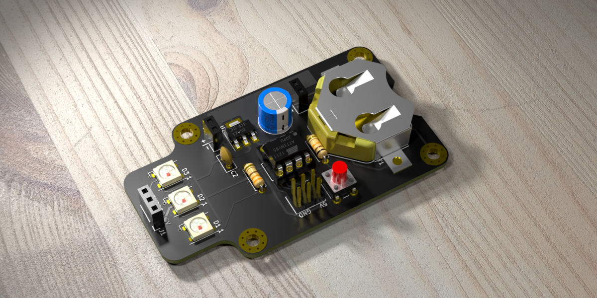
In this workshop, Anool Mahidharia takes the output of KiCad’s VRML export, gets it rendering in Blender, and then starts tweaking the result until you’re almost not sure if it’s the real thing or a 3D model. He starts off with a board in KiCad, included in the project’s GitHub repo, and you can follow along through the basic import, or go all the way to copying the graphics off the top of an ATtiny85 and making sure that the insides of the through-plated holes match the tops.

If you don’t know Blender, maybe you don’t know how comprehensive a 3D modelling and animation tool it is. And with the incredible power comes a notoriously steep learning curve up a high mountain. Anool doesn’t even try to turn you into a Blender expert, but focuses on the tweaks and tricks that you’ll need to make good looking PCB renders. You’ll find general purpose Blender tutorials everywhere on the net, but if you want something PCB-specific, you’ve come to the right place.

Continue reading “Remoticon Video: KiCad To Blender PCB Renders”

Logitech Joystick Gets A Mechanical Sidekick

The mechanical keyboard rabbit hole is a deep one, and can swallow up as much money and time as you want to spend. If you’ve become spoiled on the touch and responsiveness of a Cherry MX or other mechanical switch, you might even start putting them on other user interfaces as well, such as this Logitech joystick that now sports a few very usable mechanical keys for the touch-conscious among us.

The Logitech Extreme 3D Pro that [ErkHal] and friend [HeKeKe] modified to accept the mechanical keys originally had a set of input buttons on the side, but these were unreliable and error-prone with a very long, inconsistent push. Soldering some mechanical switches directly on the existing board was a nice improvement, but the pair decided that they could do even better and rolled out an entire custom PCB to mount the keys more ergonomically. The switches are Kailh Choc V2 Browns and seem to have done a great job of improving the responsiveness of the joystick’s side buttons. If you want to spin up your own version, they’ve made the PCBs available on their GitHub page.

While [ErkHal] notes the switches aren’t the best and were only used since they were available, they certainly appear to work much better than what the joystick shipped with originally. In fact, we recently saw similar switches used to make a custom mechanical keyboard made for the PinePhone.

Printed Circuits, 1940s Style

A presentation this month by the Antique Wireless Museum brought British engineer and inventor John Sargrove (1906-1974) to our attention. If you’ve ever peeked inside old electronics from days gone by, you’ve no doubt seen point-to-point wiring and turret board construction. In the 60s and 70s these techniques eventually made way for printed circuit boards which we still use today. But Mr Sargrove was way ahead of his time, having already invented a process in the 1930s to print circuits, not just boards, onto Bakelite. After being interrupted by the war, he formed a company Electronic Circuit Making Equipment (ECME) and was building broadcast radio receivers on an impressive automatic production line.

Mr. Sargrove’s passion was making radios affordable for everyone. But to achieve this goal, he had to make large advances manufacturing technology. His technique of embedding not only circuit traces, but basic circuit elements like resistors, capacitors, and inductors directly into the substrate foresaw techniques being applied decades later in integrated circuit design.  He also developed a compact vacuum tube which could be used in all circuits of a radio, called an “All-stage Valve“. Equally important was his futuristic automatic factory, which significantly reduced the number of factory workers needed to make radios from 1500 to 50. Having completed the radio design, he was also developing a television receiver using the same concepts. Unfortunately, ECME was forced into liquidation when a large order from India was cancelled upon declaration of independence in 1947.

You really must watch the video below. There are many bits and pieces of modern factory automation which we still use today, yet their implementation using 1940s techniques and technology is fascinating. Further reading links after the video. Thanks to [Mark Erdle] for the tip.

Continue reading “Printed Circuits, 1940s Style”

Remoticon Video: How To Reverse Engineer A PCB

You hold in your hand a circuit board from a product you didn’t make. How does the thing work? What a daunting question, but it’s both solvable and approachable if you know what you’re doing. The good news is that Eric Schlaepfer knows exactly what he’s doing and boiled down the process of reverse engineering printed circuit boards into this excellent workshop. It was presented live during the 2020 Hackaday Remoticon, and the edited video, which you’ll find below, was just published. Slides for the talk have been published on the workshop project page.

Need proof that he has skills that we all want? Last year Eric successfully reverse-engineered the legendary Sound Blaster audio card and produced his own fully-functional drop-in replacement called the Snark Barker. And then re-engineered it to work with the ancient MCA bus architecture. Whoa.

Continue reading “Remoticon Video: How To Reverse Engineer A PCB”

Get Over Your Fears

Some projects are just too complex, that’s for sure. But I’d be willing to bet that some things you think are too difficult actually aren’t, and it may be that all you need to get over your personal hurdle is a good demonstration. Here come three cases in point.

I was looking at the new Raspberry Pi Compute Module last weekend. They have a whole bunch of high-speed traces: things like Gigabit Ethernet, HDMI, and those crazy-fast SDI serial camera interfaces. I have no experience in high-speed design and layout at all, and frankly it gives me the willies. But the Raspberries also shipped me an IO demo board, and concomitant KiCAD design files, with the review board. Looking at it, they were just wires — maybe pairwise length-matched and impedance controlled — but also just wires. Opening up the KiCAD board file and clicking on the traces just like I do with my own designs, I’m a lot less scared. That was a revelation for me.

In a great writeup of his experience building ten different Linux single-board-computers from scratch, Jay Carlson had a similar effect on me. I would never have considered breaking out the hotplate for some CPU-and-DRAM action, and I’ve never had to lay out a PCB with a high density BGA chip before either. I’m not quite into Dunning-Kruger territory yet; I still have a healthy respect for the layout intricacies in fanning out a tight BGA CPU into a DRAM. But Jay’s frank assessments of what is easy and what is hard make it all seem within the realm of the doable.

As Mike and I were talking on the podcast about Jay’s work, Mike came clean about his fear of BGAs. I’ve done enough reflow-plate soldering, with parts that have a lead pitch that’s a factor of two finer than the 0.8 mm pitch BGAs in question, so it doesn’t seem implausible to me. And I’m 100% sure Mike could pull it off too, but he is in need of a BGA guru. Any good hobbyist videos out there?

Being a nerdy type, I’m much more focused on the knowledge and the inspiration, but maybe the courage is equally important — at least I think I undervalue it. I don’t need to lay out HDMI lines, or build a from-scratch Linux box, but I am no longer afraid that I couldn’t, and that’s because I’ve seen detailed examples of fellow hackers who’ve done the same. I might not get it right on the first shot, but I’m not afraid to try, and I wouldn’t have said the same before looking over other folks’ shoulders. Forza e corragio!

Let KiCad And Python Make Your Coils

We like to pretend that our circuits are as perfect as our schematics. But in truth, PCB traces have unwanted resistance, capacitance, and inductance. On the other hand, that means you can use those traces to build components. For example, it isn’t uncommon to see a very small value current sense resistor be nothing more than a long PC board trace. Using PC layers for decoupling capacitance and creating precise transmission lines are other examples. [IndoorGeek] takes us through his process of creating coils on the PCB using KiCad. To help, he used a Python script that works out the circles, something KiCAD has trouble with.

The idea is simple. A coil of wire has inductance even if it is a flat copper trace on a PCB. In this case, the coils are more for the electromagnetic properties, but the same idea applies if you wanted to build tuned circuits. The project took inspiration from FlexAR, an open-source flexible PCB magnet.

Continue reading “Let KiCad And Python Make Your Coils”

Put That New Resin Printer To Work Making PCBs

With all the cool and useful parts you can whip up (relatively) quickly on a 3D printer, it’s a shame you can’t just print a PCB. Sure, ordering a PCB is quick, easy, and cheap, but being able to print one-offs would peg the needle on the instant gratification meter.

[Peter Liwyj] may just have come up with a method to do exactly that. His Instructables post goes into great detail about his method, which uses an Elegoo Mars resin printer and a couple of neat tricks. First, a properly cleaned board is placed copper-side down onto a blob of SLA resin sitting on the print bed. He tricks the printer into thinking the platform is all the way down for the first layer by interrupting the photosensor used to detect home. He lets the printer go through one layer of an STL file that contains his design, which polymerizes a thin layer of plastic onto the copper. The excess resin is wiped gently away and the board goes straight into a ferric chloride etching bath. The video below shows the whole process.

As simple as it sounds, it looks like it works really well. And [Peter] didn’t just stumble onto this method; he approached it systematically and found what works best. His tips incude using electrical tape as a spacer to lift the copper off the print surface slightly, cleaning the board with Scotchbrite rather than sandpaper, and not curing the resin after printing. His toolchain is a bit uncoventional — he used SketchUp to create the traces and exported the STL. But there are ways to convert Gerbers to STLs, so your favorite EDA package can probably fit in to the process too.

Don’t have a resin printer? Don’t worry — FDM printers can work too.

Continue reading “Put That New Resin Printer To Work Making PCBs”