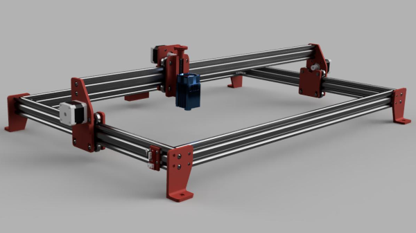
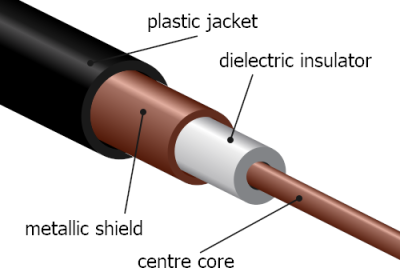
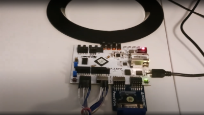
This modern era of GPU-accelerated AI applications have their benefits. Pulling useful information out of mountains of raw data, alerting users to driving hazards, or just keeping an eye on bee populations are all helpful. Lately there has been a rise in attempts at producing (or should that be curating?) works of art out of carefully sculpted inputs.
One such AI art project is midjourney, which can be played with via a Discord integration bot. That bot takes some textual input, then “dreams” with it, producing sometime uncanny, often downright disturbing images.
We’re going to go out on a limb and predict that future history books will note that the decision to invade a sovereign nation straight after a worldwide pandemic wasn’t exactly the best timing. Turns out the global electronics shortage the pandemic helped to catalyze isn’t just affecting those of us with peaceful intentions, as the Russian war machine is having a few supply issues with the parts needed to build modern weapons and their associated control equipment.
As you might expect, many of these parts are electronic in nature, and in some cases they come from the same suppliers folks like us use daily. This article from POLITICO includes an embedded spreadsheet, broken down by urgency, complete with part numbers, manufacturers, and even the price Moscow expects to pay!
Chips from US-based firms such as Texas Instruments are particularly hard for the Kremlin to source.
So what parts are we talking about anyway? The cheapest chip on the top priority list is the Marvell ‘Alaska’ 88E1322 which is a dual Gigabit Ethernet PHY costing a mere $7.10 USD according to Moscow. The most expensive is the 10M04DCF256I7G, which is an Altera (now Intel) Max-10 series FPGA, at $1,101 USD (or 66,815 Rubles, for those keeping score).
But it’s not just chips that are troubling them, mil-spec D-sub connectors by Airborn are unobtainable, as are all classes of basic passive parts, resistors, diodes, discrete transistors. Capacitors are especially problematic (aren’t they always). A whole slew of Analog Devices chips, as well as many from Maxim, Micrel and others. Even tiny logic chips from Nexperia.
Of course, part of this is by design. Tightened sanctions prevent Russia from purchasing many of these parts directly, which is intended to make continued aggression as economically unpleasant as possible. But as the POLITICO article points out, it’s difficult to prevent some intermediaries from ‘helping out’ without the West knowing. After all, once a part hits the general market, it is next to impossible to guarantee where it will eventually get soldered down.
PCB design starts off being a relatively easy affair — you create a rectangular outline, assign some component footprints, run some traces, and dump out some Gerber files to send to the fab. Then as you get more experienced and begin trying harder circuits, dipping into switching power supplies, high speed digital and low noise analog, things get progressively more difficult; and we haven’t even talked about RF or microwave design yet, where things can get just plain weird from the uninitiated viewpoint. [Robert Feranec] is no stranger to such matters, and he’s teamed up with one of leading experts (and one of this scribe’s personal electronics heroes) in signal integrity matters, [Prof. Eric Bogatin] for a deep dive into the how and why of controlled impedance design.
RG58 cable construction. These usually are found in 50 Ω and less commonly these days 75Ω variants
One interesting part of the discussion is why is 50 Ω so prevalent? The answer is firstly historical. Back in the 1930s, coaxial cables needed for radio applications, were designed to minimize transmission loss, using reasonable dimensions and polyethylene insulation, the impedance came out at 50 Ω. Secondarily, when designing PCB traces for a reasonable cost fab, there is a trade-off between power consumption and noise immunity.
As a rule of thumb, lowering the impedance increases noise immunity at the cost of more power consumption, and higher impedance goes the other way. You need to balance this with the resulting trace widths, separation and overall routing density you can tolerate.
Another fun story was when Intel were designing a high speed bus for graphical interfaces, and created a simulation of a typical bus structure and parameterized the physical constants, such as the trace line widths, dielectric thickness, via sizes and so on, that were viable with low-cost PCB fab houses. Then, using a Monte Carlo simulation to run 400,000 simulations, they located the sweet spot. Since the via design compatible with the cheap fab design rules resulted often in a via characteristic impedance that came out quite low, it was recommended to reduce the trace impedance from 100 Ω to 85 Ω differential, rather than try tweak the via geometry to bring it up to match the trace. Fun stuff!
We admit, the video is from the start of the year and very long, but for such important basic concepts in high speed digital design, we think it’s well worth your time. We certainly picked up a couple of useful titbits!
Now we’ve got the PCB construction nailed, why circle back and go check those cables?
Stored hydrogen is often touted as the ultimate green energy solution, provided the hydrogen is produced from genuinely green power sources. But there are technical problems to be overcome before your average house will be heated with pumped or tank-stored hydrogen. One problem is that the locations that have lots of scope for renewable energy, don’t always have access to plenty of pure water, and for electrolysis you do need both. A team from Melbourne University have come up with a interesting way to produce hydrogen by electrolysis directly from the air.
Redder areas have more water risk and renewable potential
By utilising a novel electrolysis cell with a hygroscopic electrolyte, the so-called direct air electrolysis (DAE) can operate with humidity as low as 4% relative, so perfectly fine even in the most arid areas, after all there may not be clouds but the air still holds a bit of water. This is particularly relevant to regions of the world, such as deserts, where there is simultaneously a high degree of water risk, and plenty of solar potential. Direct electrolysis of saline extracted at coastal areas is one option, but dealing with the liberated chlorine is a big problem.
The new prototype is very simple in construction, with a sponge of melamine or a sintered glass foam soaked in a compatible electrolyte. Potassium Hydroxide (alkaline) was tried as was Potassium Acetate (base) and Sulphuric Acid, but the latter degraded the host material in a short time. Who would have imagined? Anyway, with electrolysis cell design, a key problem is ensuring the separate gasses stay separate, and in this case, are also separate from the air. This was neatly ensured by arranging the electrolyte 
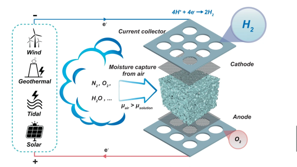
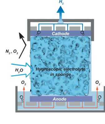
sponge fully covered both electrodes, so as the hygroscopic material extracted water from the air, the micro-channels in the structure filled up with liquid, with it touching both ends of the cell, forming the circuit and allowing the electrolysis to proceed.
Hydrogen, being very light, would rise upward through holes in the cathode, to be collected and stored. Oxygen simply passed back into the air, after passing though the liquid reservoir at the base. Super simple, and from reading the paper, quite effective too.
You can kind of imagine a future built around this now, where you’re driving your hydrogen fuel cell powered dune buggy around the Sahara one weekend, and you stop at a solar-powered hydrogen fuel station for a top up and a pasty. Ok, possibly not that last bit.
[Vuong Nguyen] clearly knows his way around artificial intelligence accelerator hardware, creating ztachip: an open source implementation of an accelerator platform for AI and traditional image processing workloads. Ztachip (pronounced “zeta-chip”) contains an array of custom processors, and is not tied to one particular architecture. Ztachip implements a new tensor programming paradigm that [Vuong] has created, which can accelerate TensorFlow tasks, but is not limited to that. In fact it can process TensorFlow in parallel with non-AI tasks, as the video below shows.
A RISC-V core, based on the VexRiscV design, is used as the host processor handling the distribution of the application. VexRiscV itself is quite interesting. Written in SpinalHDL (a Scala variant), it’s super configurable, producing a Verilog core, ready to drop into the design.
A Digilent Arty-A7, Arducam and a VGA PMOD is all you need
From a hardware design perspective the RISC-V core hooks up to an AXI crossbar, with all the AXI-lite busses muxed as is usual for the AMBA AXI ecosystem. The Ztachip core as well as a DDR3 controller are also connected, together with a camera interface and VGA video.
Other than providing an FPGA-specific DDR3 controller and AXI crossbar IP, the rest of the design is generic RTL. This is good news. The demo below deploys onto an Artix-7 based Digilent (Arty-A7) with a VGA PMOD module, but little else needed. Pre-build Xilinx IP is provided, but targeting a different FPGA shouldn’t be a huge task for the experienced FPGA ninja.
Ztachip top level architecture
The magic happens in the Ztachip core, which is mostly an array of Pcores. Each Pcore has both vector and scalar processing capability, making it super flexible. The Tensor Engine (internally this is the ‘dataplane processor’) is in charge here, sending instructions from the RISC-V core into the Pcore array together with image data, as well as streaming video data out. That camera is only a 0.3 MP Arducam, and the video is VGA resolution, but give it a bigger FPGA and those limits could be raised.
This domain-specific approach uses a highly modified C-like language (with a custom compiler) to describe the application that is to be distributed across the accelerator array. We couldn’t find any documentation on this, but there are a few example algorithms.
The demo video shows a real-time mix of four algorithms running in parallel; one object classification (Google’s Tensorflow mobilenet-ssd, a pre-trained AI model) canny edge detection, a Harris corner detection, and Optical flow which gives it a predator-like motion vision.
[Vuong] reckons, efficiency wise it is 5.5x more computationally efficient than a Jetson Nano and 37x more than Google’s TPU edge. These are bold claims, to say the least, but who are we to argue with a clearly incredibly talented engineer?
[Neumi] over on Hackaday.IO wanted a simple-to-use way to drive stepper motors, which could be quickly deployed in a wide variety of applications yet to be determined. The solution is named Ethersweep, and is a small PCB stack that sits on the rear of the common NEMA17-format stepper motor. The only physical connectivity, beside the motor, are ethernet and a power supply via the user friendly XT30 connector. The system can be closed loop, with both an end-stop input as well as an on-board AMS AS5600 magnetic rotary encoder (which senses the rotating magnetic field on the rear side of the motor assembly – clever!) giving the necessary feedback. Leveraging the Trinamic TMC2208 stepper motor driver gives Ethersweep silky smooth and quiet motor control, which could be very important for some applications. A rear-facing OLED display shows some useful debug information as well as the all important IP address that was assigned to the unit.
Control is performed with the ubiquitous ATMega328 microcontroller, with the Arduino software stack deployed, making uploading firmware a breeze. To that end, a USB port is also provided, hooked up to the uC with the cheap CP2102 USB bridge chip as per most Arduino-like designs. The thing that makes this build a little unusual is the ethernet port. The hardware side of things is taken care of with the Wiznet W5500 ethernet chip, which implements the MAC and PHY in a single device, needing only a few passives and a magjack to operate. The chip also handles the whole TCP/IP stack internally, so only needs an external SPI interface to talk to the host device.
Some people may have heard of Dutch programmer [Wouter Van Oortmerssen] since he’s the creator of the Amiga-E programming language, as well as being involved with several game engines. Heard of SimCity? How about Borderlands 2 or Far Cry? Having had clearly a long and illustrious career as a programmer for a variety of clients — including a long stint at Google, working on Web Assembly — many people will be familiar with at least some of his work. But you may not have heard of his TreeSheets productivity tool. Which would be a shame, as you’ve been missing out on something pretty darn useful.
TreeSheets is described as a hierarchical spreadsheet, which is intended as a replacement for several distinct tools; think spreadsheets, mindmaps and text editors and similar. In [Wouter]’s words:
It’s like a spreadsheet, immediately familiar, but much more suitable for complex data because it’s hierarchical.
It’s like a mind mapper, but more organized and compact.
It’s like an outliner, but in more than one dimension.
It’s like a text editor, but with structure.
Having been in development for about a decade, TreeSheets might look a bit dated here and there, but the design is clear and distraction-free, which is exactly what you need when you’re trying to focus on the task in hand. Why not give it a try and see if it works for you? After the break, you can see a video tutorial by YouTube user [DrilixProject].