JavaScript App Uses Advanced Math To Make PCBs Easier To Etch

We all remember the litany from various math classes we’ve taken, where frustration at a failure to understand a difficult concept bubbles over into the classic, “When am I ever going to need to know this in real life?” But as we all know, even the most esoteric mathematical concepts have applications in the real world, and failure to master them can come back to haunt you.

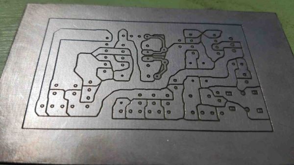
Take Voronoi diagrams, for example. While we don’t recall being exposed to these in any math class, it turns out that they can be quite useful in a seemingly unrelated area: converting PCB designs into easy-to-etch tessellated patterns. Voronoi diagrams are in effect a plane divided into different regions, or “cells”, each centered on a “seed” object. Each cell is the set of points that are closer to a particular seed than they are to any other seed. For PCBs the seeds can be represented by the traces; dividing the plane up into cells around those traces results in a tessellated pattern that’s easily etched.

To make this useful to PCB creators, [Craig Iannello] came up with a JavaScript application that takes an image of a PCB, tessellates the traces, and spits out G-code suitable for a laser engraver. A blank PCB covered with a layer of spray paint, the tessellated pattern is engraved into the paint, and the board is etched and drilled in the usual fashion. [Craig]’s program makes allowances for adding specific features to the board, like odd-shaped pads or traces that need specific routing.

This isn’t the first time we’ve seen Voronoi diagrams employed for PCB design, but the method looks so easy that we’d love to give it a try. It even looks as though it might work for CNC milling of boards too.
PCB Bath Comes From Russia With Love

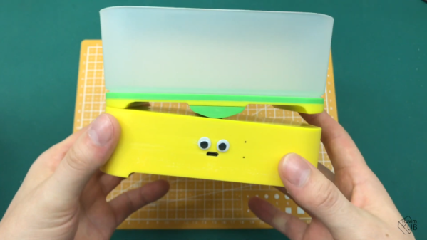
[Ruvin Kub] likes magnets, a lot. Most of his projects feature some sort of magnet and his PC board agitation bath is no exception. You can see a video about the device, below. We’ll admit our Russian is pretty rusty, but if you ask YouTube nicely it will translate the Russian subtitles into whatever language you like.

One of the things we liked about the video was that he uses hydrogen peroxide, citric acid, and salt as an etchant. We’ve seen the same mix with vinegar or muriatic acid instead of citric acid. We aren’t sure what the actual  translation is about why he doesn’t like ferric chloride, but YouTube says, “she’s too gloomy for my light souls.”

Continue reading “PCB Bath Comes From Russia With Love”

Laser Blasts Out High-Quality PCBs

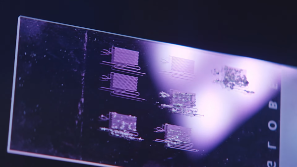
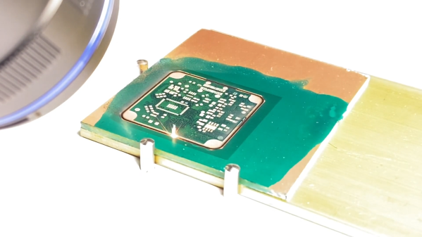
With how cheap and how fast custom PCBs have gotten, it almost doesn’t make sense to roll your own anymore, especially when you factor in the messy etching steps and the less than stellar results. That’s not the only way to create a PCB, of course, and if you happen to have access to a 20-Watt fiber laser, you can get some fantastic homemade PCBs that are hard to tell from commercial boards.

Lucikly, [Saulius Lukse] of Kurokesu fame has just such a laser on hand, and with a well-tuned toolchain and a few compromises, he’s able to turn out 0.1-mm pitch PCBs in 30 minutes. The compromises include single-sided boards and no through-holes, but that should still allow for a lot of different useful designs. The process starts with Gerbers going through FlatCAM and then getting imported into EZCAD for the laser. There’s a fair bit of manual tweaking before the laser starts burning away the copper between the traces, which took about 20 passes for 0.035-mm foil on FR4. We have to admit that watching the cutting proceed in the video below is pretty cool.

Once the traces are cut, UV-curable solder resist is applied to the whole board. After curing, the board goes back to the laser for another pass to expose the pads. A final few passes with the laser turned up to 11 cuts the finished board free. We wonder why the laser isn’t used to drill holes; we understand that vias would be hard to connect to the other side, but it seems like through-hole components could be supported. Maybe that’s where [Saulius] is headed with this eventually, since there are traces that terminate in what appears to be via pads.

Whatever the goal, these boards are really slick. We usually see lasers used to remove resist prior to traditional etching, so this is a nice change.

Continue reading “Laser Blasts Out High-Quality PCBs”

Micromachining Glass With A Laser — Very, Very Slowly

When it comes to machining, the material that springs to mind is likely to be aluminum, steel, or plastic. We don’t necessarily think of glass as a material suitable for machining, at least not in the chuck-it-up-in-the-lathe sense. But glass is a material that needs to be shaped, too, and there are a bunch of different ways to accomplish that. Few, though, are as interesting as micromachining glass with laser-induced plasma bubbles. (Video, embedded below.)

The video below is from [Zachary Tong]. It runs a bit on the longish side, but we found it just chock full of information. The process, formally known as “laser-induced backside wet-etching,” uses a laser to blast away at a tank of copper sulfate. When a piece of glass is suspended on the surface of the solution and the laser is focused through the glass from the top, some interesting things happen.

The first pulse of the laser vaporizes the solution and decomposes the copper sulfate. Copper adsorbs onto the glass surface inside the protective vapor bubble, which lasts long enough for a second laser pulse to come along. That pulse heats up the adsorbed copper and the vapor in the original bubble, enough to melt a tiny bit of the glass. As the process is repeated, small features are slowly etched into the underside of the glass. [Zachary] demonstrates all this in the video, as well as what can go wrong when the settings are a bit off. There’s also some great high-speed footage of the process that’s worth the price of admission alone.

We doubt this process will be a mainstream method anytime soon, not least because it requires a 50-Watt Nd:YAG fiber laser. But it’s an interesting process that reminds us of [Zachary]’s other laser explorations, like using a laser and Kapton to make graphene supercapacitors.

Continue reading “Micromachining Glass With A Laser — Very, Very Slowly”

Hackaday Links Column Banner

Hackaday Links: September 13, 2020

Like pretty much every other big conference, the Chaos Communication Conference is going virtual this year. What was supposed to be 37C3 has been rebranded as rC3, the remote Chaos Experience. It’s understandable, as a 17,000 person live event would have not only been illegal but a bit irresponsible in the current environment. The event appears to be a hybrid of small local events hosted in hackerspaces linked with streamed talks and a program of workshops and “online togetherness.” rC3 is slated to run in the week between Christmas and New Year, and it seems like a great way to wrap up 2020.

Speaking of remote conferences, don’t forget about our own Remoticon. While it won’t be quite the same as everyone getting together in sunny — historically, at least — Pasadena for a weekend of actual togetherness, it’s still going to be a great time. The event runs November 6 to 8; we’ve had a sneak peek at the list of proposed workshops and there’s some really cool stuff. Prepare to be dazzled, and make sure you keep up on the Remoticon announcements — you really don’t want to miss this.

Continue reading “Hackaday Links: September 13, 2020”

Transform Kicad Design To Patchwork For Isolation Routing

Tuning a desktop router and your board designs for isolation routing can be a bit tricky, with thin traces usually being the first victim. For simple prototype boards you usually don’t need tightly packed traces, you just want to isolate the nets. To do this with a minimum amount of routing, [Michael Schembri] created kicad-laser-min, a command-line utility that takes a Kicad PCB design and expands all the tracks and pads to their maximum possible width.

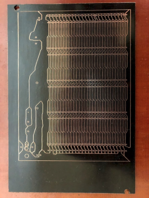
Laser scribed PCB with maximum track widths

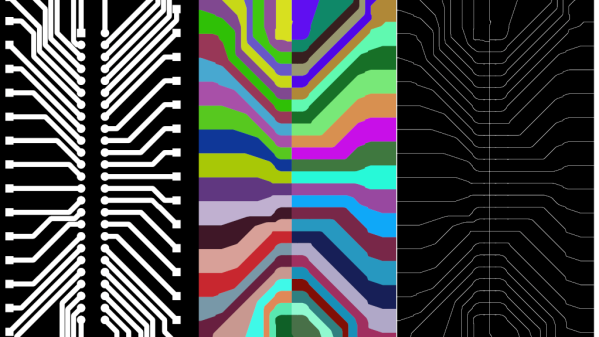
The software takes one layer of the PCB layout, converts it to black and white, and then runs a C++ Voronoi algorithm on it to dilate each track and pad until it meets another expanding region. Each region is colourised, and OpenCV edge detection is used to produce the contours that need to be milled or etched. A contour following algorithm is then used to create the G-code. The header image shows the output of each step.

Full source code is available on GitHub. [Michael] has had good results with his own boards, which are scribed using a laser cutter before etching, but welcomes testing and feedback from other users. He has found that OpenCV doesn’t always completely close all the contours, but the gaps are usually smaller than the engraving width of his laser, so no shorts are created.

This is basically “Scribble style” prototyping with CAD and CNC tools. If you prefer scribe and etch, you might consider building a simple PCB shaker for faster etching. If you have a router but want to avoid the dust, you can use a carbide scribe to scratch out the tracks without needing to etch.

Making PCBs The Easy Way

Building a PCB at home can be fraught. If you’re etching, there are chemicals and the nuances of toner transfer. If you’re milling, getting the surface height just right, and not breaking those pointy little v-cutters is always a challenge. [Robin] has tips for both of these cases, and solves a lot of the common hassles by using a milling machine.

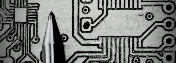
Whether he’s scraping away etch resist or entire copper isolation lines, [Robin] uses a non-spinning scratching tool instead of a v-bit: they’re more robust and cut every bit as well. He’s got tips for using FlatCam and KiCAD to make scratched-out traces. His registration system allows him to get double-sided boards with a minimum of hassle. And as a bonus, he’s doing some experimentation with embedding SMT parts inside the boards as well. Be sure that you check out his whole guide, or just watch the video embedded below.

We’re pretty sure you’ll pick up a trick or two, and maybe you’ll be convinced to bite the bullet and invest in a nice mill. If you’d like a more traditional take on PCB milling, try out our own [Adil Malik]’s guide.

Continue reading “Making PCBs The Easy Way”